
Nanoscale relaxation oscillator

a relaxation oscillator and nanoscale technology, applied in the field of nanostructures, can solve the problems of limited degree to which surface tension is exploited by these approaches, and the inherently unidirectional nature of surface tension action, and achieve the effect of significant mechanical for

Inactive Publication Date: 2009-04-07
RGT UNIV OF CALIFORNIA
View PDF3 Cites 2 Cited by
  • Summary
  • Abstract
  • Description
  • Claims
  • Application Information

AI Technical Summary

Benefits of technology

The present invention is about a mechanical relaxation oscillator device that operates on a nanometer scale. It uses two nanoparticles that are connected by a channel for conducting atomic mass transfer and supporting particle growth. The particles are liquid at no more than a slight elevated temperature, and they have a low vapor pressure near their melting point. The channel is a nanotube, single or multiwalled carbon nanorod, wire, or a quasi-one dimensional path on a two-dimensional surface. The actuator, which transmits the oscillation, may be another nanotube or a small piece of metal in movable contact with the droplet. The device can be powered by a simple, non-modulating power output, such as a battery or solar cell connected directly to the electrodes. The oscillator can be used in various applications, such as generating electromagnetic radiation or sound waves. The slow and fast phases of oscillation are caused by atomic mass transport and surface tension, respectively.

Problems solved by technology

The degree to which surface tension is exploited by these approaches is limited, however.
In the other cases, the surface tension action is inherently unidirectional.

Method used


Image

  • Nanoscale relaxation oscillator
  • Nanoscale relaxation oscillator
  • Nanoscale relaxation oscillator

Examples


Embodiment Construction

Definitions

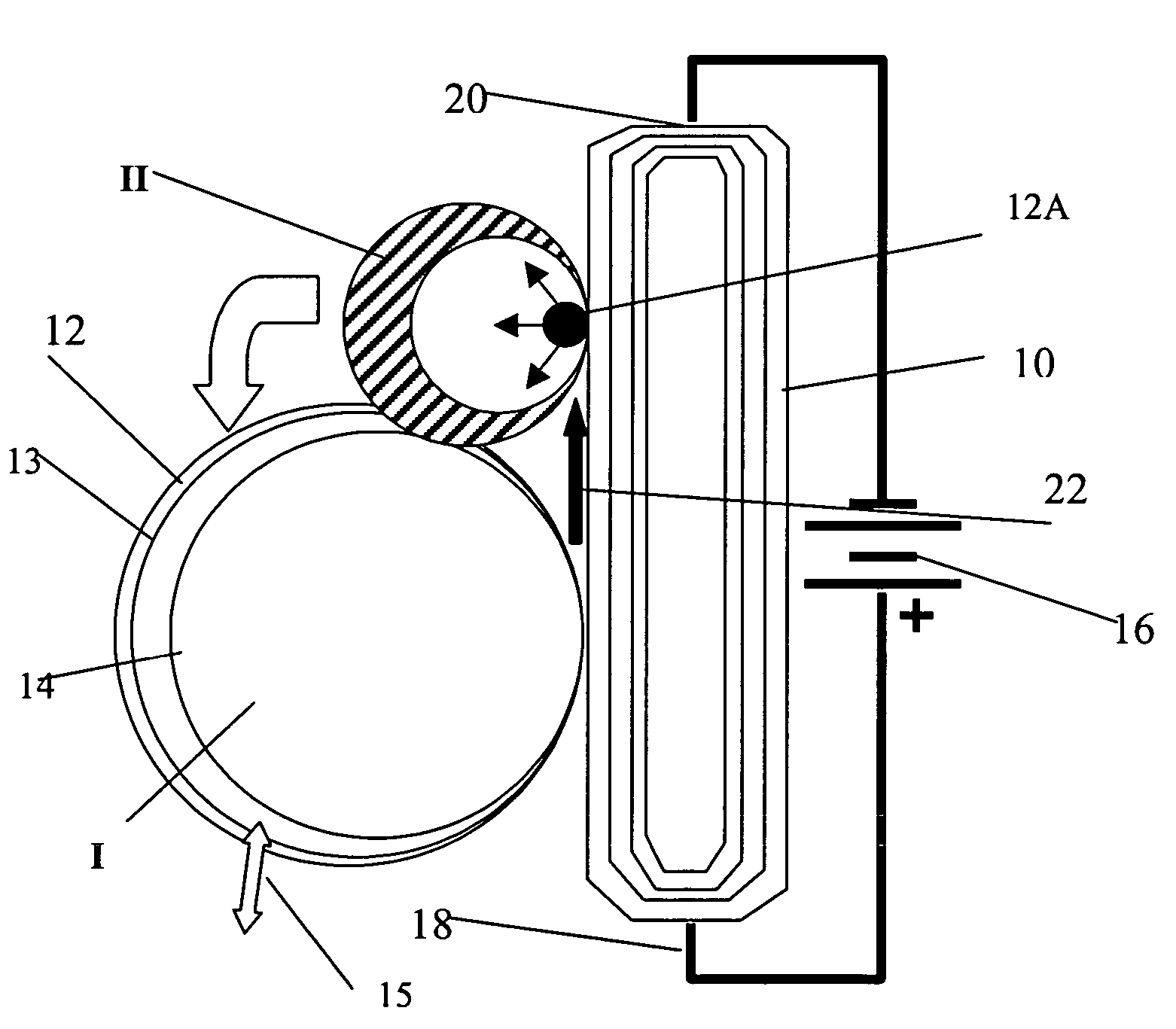
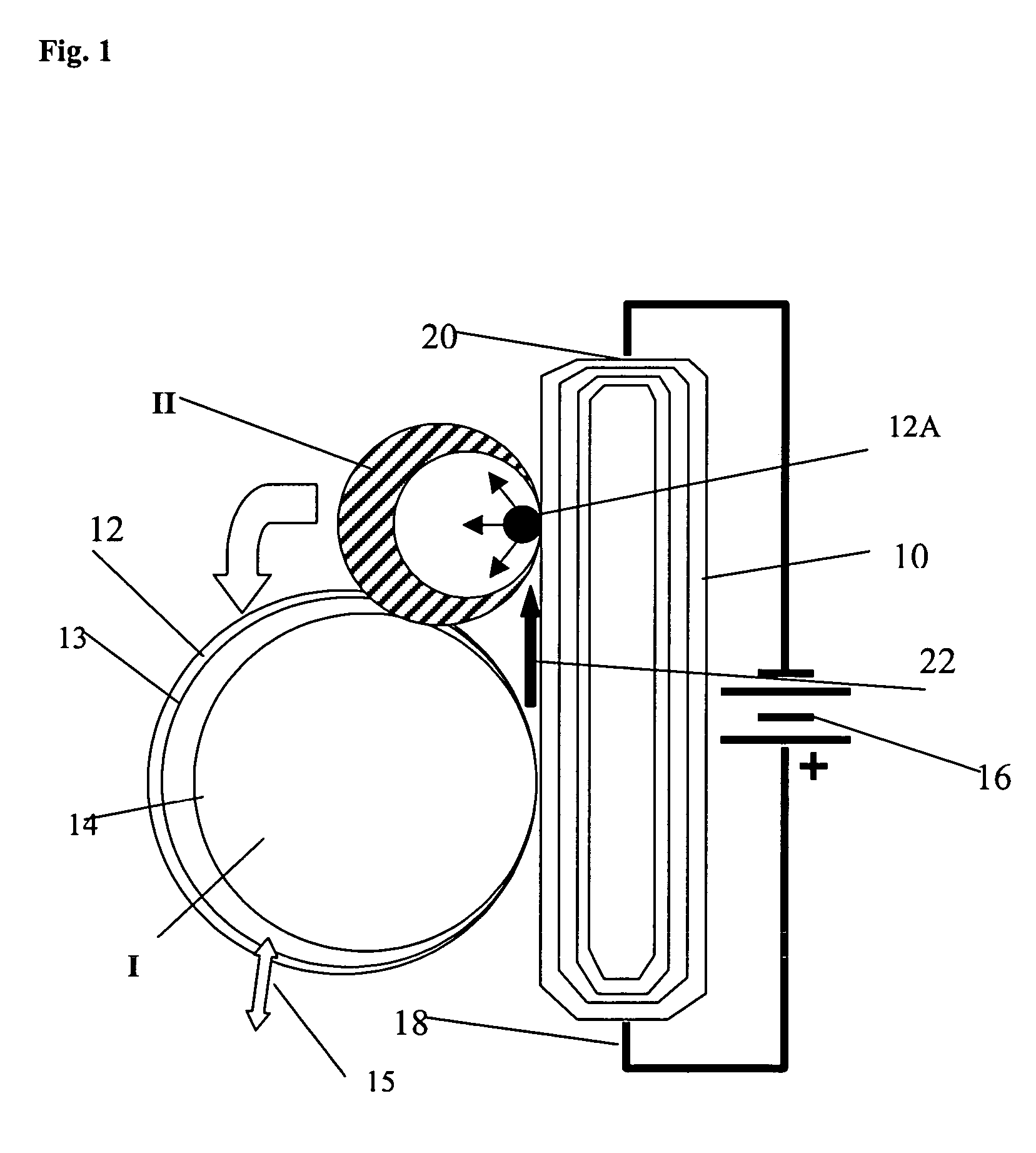
[0033]The term “channel” is used herein in its most general sense. It is intended to cover nanotubes (single or multiwalled, made of various materials such as carbon or boron nitride), nanorods, nanowires, quasi-one dimensional paths on two-dimensional surfaces that are defined by chemical or physical means (i.e. by treating the surface to create a barrier to unconstrained two-dimensional surface diffusion), and the like. A silicon wafer may be etched with a fine groove to provide the present channel. The channel is essentially atomically smooth, as that term is understood in the field of material science. As used herein, and generally understood in the art, “atomically smooth” means lacking in contaminants, imperfections or other barriers, cavities or defects that disrupt an ordered atomic structure that would provide an extremely smooth surface. A discussion of atomic smoothness is found in Koch et al., “Modelling of HREM and nanodiffraction for dislocation kinks and co...


PUM


Abstract

A nanoscale oscillation device is disclosed, wherein two nanoscale droplets are altered in size by mass transport, then contact each other and merge through surface tension. The device may also comprise a channel having an actuator responsive to mechanical oscillation caused by expansion and contraction of the droplets. It further has a structure for delivering atoms between droplets, wherein the droplets are nanoparticles. Provided are a first particle and a second particle on the channel member, both being made of a chargeable material, the second particle contacting the actuator portion; and electrodes connected to the channel member for delivering a potential gradient across the channel and traversing the first and second particles. The particles are spaced apart a specified distance so that atoms from one particle are delivered to the other particle by mass transport in response to the potential (e.g. voltage potential) and the first and second particles are liquid and touch at a predetermined point of growth, thereby causing merging of the second particle into the first particle by surface tension forces and reverse movement of the actuator. In a preferred embodiment, the channel comprises a carbon nanotube and the droplets comprise metal nanoparticles, e.g. indium, which is readily made liquid.

Description

CROSS-REFERENCE TO RELATED APPLICATIONS[0001]This application claims benefit of Provisional Patent Application Ser. No. 60 / 617,583 filed Oct. 8, 2004, patent application Ser. No. 11 / 085,397, filed Mar. 21, 2005, by the same inventors, entitled “Nanoscale Mass Conveyor,” and patent application Ser. No. 11 / 229,935 filed Sep. 19, 2005 entitled “Nanocrystal Powered Nanomotor,” also naming the same inventors. These applications are hereby incorporated by reference into the present application.STATEMENT OF GOVERNMENTAL SUPPORT[0002]This invention was made during work supported by U.S. Department of Energy under Contract No. DE-AC02-05CH11231 and National Science Foundation Grant CCR 0210176. The government has certain rights in this invention.REFERENCE TO SEQUENCE LISTING OR COMPACT DISK[0003]NONEBACKGROUND OF THE INVENTION[0004]1. Field of the Invention[0005]The present invention relates to the field of nanostructures, to oscillators, and to the application of mass transport and hydrodyn...

Claims


Application Information

Patent Timeline
Patent Type & Authority Patents(United States)
IPC IPC(8): H03B5/30
CPCB82Y10/00B82Y15/00H02N11/006Y10S977/962Y10S977/725
Inventor ZETTL, ALEXANDER K.REGAN, BRIAN C.ALONI, SHAUL
Owner RGT UNIV OF CALIFORNIA
Learn More