Bit line voltage supply circuit in semiconductor memory device and voltage supplying method therefor

a voltage supply circuit and semiconductor memory technology, applied in information storage, static storage, digital storage, etc., can solve the problems of limitation on the reduction of standby current in a standby mode by means of conventional methods, and conventional methods do not reduce leakage current, so as to reduce current consumption and without substantially deteriorating the device characteristics

Active Publication Date: 2009-03-03
SAMSUNG ELECTRONICS CO LTD +1
View PDF9 Cites 5 Cited by
  • Summary
  • Abstract
  • Description
  • Claims
  • Application Information

AI Technical Summary

Benefits of technology

[0014]The present invention provides a semiconductor memory device that reduces current consumption in a standby mode without substantially deteriorating the device characteristics.
[0015]An embodiment of the present invention provides a bit line voltage supply circuit in a semiconductor memory device and a voltage supplying method therefor, which reduce leakage current flowing through access transistors during a standby mode.
[0017]Another embodiment of the present invention provides a bit line voltage supply circuit in a semiconductor memory device and a voltage supplying method therefor, which reduce leakage current flowing through an access transistor of a memory cell and reduce wake up time with respect to an operating voltage when the semiconductor memory device changes to an operational mode.
[0018]Another embodiment of the present invention provides a method for supplying a voltage to bit lines, which applies a standby voltage as a precharge voltage of the bit lines in the case that a standby mode is held when a memory cell block is not selected, whereby a standby current may be reduced without deteriorating the operational characteristics of a device.
[0019]Another embodiment of the present invention provides an apparatus and a method, which allow a precharge voltage of bit lines to be returned to a stable operation voltage level without deteriorating operation characteristics when a semiconductor memory device changes from a standby mode to an operational mode.

Problems solved by technology

However, the conventional methods do not reduce leakage current flowing from a bit line pair BL and BLb to ground through the first and second pass transistors N3 and N4.
As a result, there is a limitation on the reduction of standby current in a standby mode by means of the conventional methods.

Method used


Image

  • Bit line voltage supply circuit in semiconductor memory device and voltage supplying method therefor
  • Bit line voltage supply circuit in semiconductor memory device and voltage supplying method therefor
  • Bit line voltage supply circuit in semiconductor memory device and voltage supplying method therefor

Examples


Embodiment Construction

[0034]Exemplary embodiments of the present invention will now be described with reference to the accompanying drawings. However, the invention should not be limited to the embodiments set forth herein. In the drawings, like numerals refer to like elements.

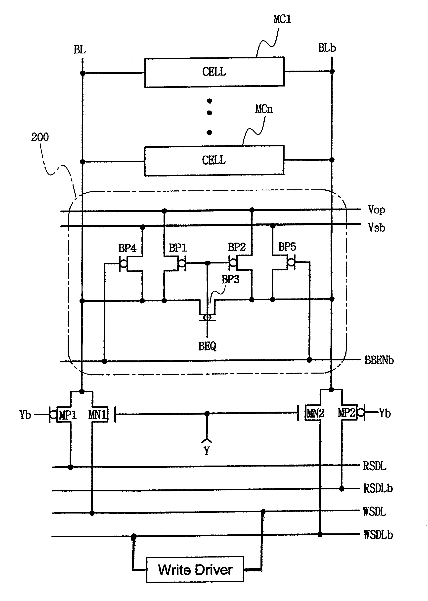
[0035]FIG. 3 is a circuit diagram showing a core cell array of a static random access memory according to an embodiment of the present invention. The core cell array of FIG. 3 differs from that of FIG. 2 with the substitution of a bit line voltage switch 200 for the similar precharge and equalization section 100.

[0036]The bit line voltage switch 200 applies a first supply (operating) voltage Vop to a bit line pair BL and BLb in response to a first bit line voltage switch control signal BEQ. The bit line voltage switch 200 applies a second supply (standby) voltage Vsb having a level lower than that of the operating voltage Vop to the bit line pair BL and BLb in response to a second bit line voltage switch control signal BBENb. The b...


PUM


Abstract

There is provided a bit line voltage supply circuit for reducing leakage current flowing from bit lines to a memory cell without substantially deteriorating the performance of a semiconductor memory device. A bit line voltage switch applies a first supply voltage to a bit line pair in response to a first switch control signal, and applies a second supply voltage having a lower voltage than the first supply voltage to the bit line pair in response to a second switch control signal. A bit line voltage controller controls the first and second switch control signals so that the second supply voltage is supplied to the bit line pair during a standby mode, and the first supply voltage is supplied to the bit line pair when the semiconductor memory device changes from the standby mode to an operational mode for a predetermined time period.

Description

CROSS-REFERENCE TO RELATED APPLICATION[0001]This application claims the benefit of Korean Patent Application No. 10-2005-0003582, filed Jan. 14, 2005, the disclosure of which is incorporated herein by reference in its entirety.BACKGROUND OF THE INVENTION[0002]1. Technical Field[0003]The present invention relates to a voltage supply for bit lines, and more particularly, to a bit line voltage supply circuit in a volatile semiconductor memory device and a voltage supplying method therefor.[0004]2. Discussion of Related Art[0005]To achieve higher performance in electronic systems such as personal computers or electronic communication devices, volatile semiconductor memory devices such as static random access memories (SRAM) are more highly integrated with higher response speed. Since semiconductor memory devices installed in battery operated systems such as hand held telephones or notebook computers benefit from low power consumption characteristics, semiconductor device manufacturers a...

Claims


Application Information

Patent Timeline
Patent Type & Authority Patents(United States)
IPC IPC(8): G11C11/00G11C5/14
CPCG11C7/12G11C11/413G11C2207/002G11C2207/005G11C5/14G11C7/06
Inventor PARK, CHUL-SUNGKIM, YOUNG-SEUNG
Owner SAMSUNG ELECTRONICS CO LTD
Why Eureka
Try Eureka