
Semiconductor laser element, manufacturing method thereof, optical disk apparatus and optical transmission system

a semiconductor laser and manufacturing method technology, applied in the field of semiconductor laser elements, can solve the problems of poor reliability of schottky junction portions, large cost increase factor in forming semiconductor laser elements, and difficulty in providing element design matched to optical characteristic specifications demanded for various applications, etc., to achieve long-term reliability, low threshold current, and high power

Inactive Publication Date: 2009-02-17
SHARP KK
View PDF10 Cites 2 Cited by
  • Summary
  • Abstract
  • Description
  • Claims
  • Application Information

AI Technical Summary

Benefits of technology

The present invention provides a semiconductor laser element that can operate with a low threshold current and high power, has long-term reliability and compatibility with cost reduction. The semiconductor laser element has a simplified manufacturing process compared to common semiconductor laser elements with buried ridge structure. The electrode layer of the semiconductor laser element forms an ohmic junction with the substrate and the second upper cladding layer, and a Schottky junction with the second conductivity type semiconductor layer. The second-conductivity-type doping concentration of the second upper cladding layer is lower than the second-conductivity-type doping concentrations of the first and third upper cladding layers, and the sum total of the layer thicknesses of the first and second upper cladding layers is not smaller than 0.3 μm but not greater than 1.5 μm. This ensures excellent current constriction and reliability with low power consumption. The semiconductor laser element can be manufactured at low cost and has increased degrees of freedom in optical characteristic design.

Problems solved by technology

However, carrying out two crystal regrowth processes is a very large cost increase factor in forming a semiconductor laser element.
However, the semiconductor laser element of JP 04-111375 A, in which the current constriction is effected by using the Schottky junction, has been unable to carry out operation with a low threshold current (e.g., 30 mA or less) and a high output power (e.g., output power exceeding 150 mW) as achieved in the conventional semiconductor laser elements of ordinary buried ridge structure.
Moreover, it has been difficult to provide an element design matched to the optical characteristic specifications demanded for various applications.
Furthermore, the Schottky junction portion has had poor reliability, and long-term reliability has not been able to be achieved.
Reasons for the failure in achieving the operation of a low threshold current and a high power may include the fact that the current constriction property at the Schottky junction portion was so insufficient that the leakage current particularly in a fine stripe-shaped structure could not be sufficiently reduced.
This has also been a factor that disturbs the high power operation.
Therefore, the degree of freedom in designing the optical characteristics has been limited.
Furthermore, no Schottky junction structure having resistance to breakdown has been disclosed, and so far there have been only structures that lack long-term reliability.
In addition, the semiconductor laser element and the manufacturing method disclosed in JP 04-111375 A has had a problem that the optical characteristics of the laser element are largely influenced by the variation in the layer thickness of the remaining p-InGaP cladding layer after etching, occasionally causing variation in the far-field pattern (FFP) in the horizontal direction and a deterioration in the stability of the transverse mode.
Furthermore, due to the variation in the InGaP layer thickness, the characteristic of the Schottky junction formed on that layer may also vary, and this may lead to an insufficient current constriction.
Thus, the degree of freedom of design is small.
There is a further problem that use of InGaP for the p-cladding layer tends to increase ΔEv, which may result in a limit to the injection efficiency of holes into the active layer.

Method used


Image

  • Semiconductor laser element, manufacturing method thereof, optical disk apparatus and optical transmission system
  • Semiconductor laser element, manufacturing method thereof, optical disk apparatus and optical transmission system
  • Semiconductor laser element, manufacturing method thereof, optical disk apparatus and optical transmission system

Examples


first embodiment

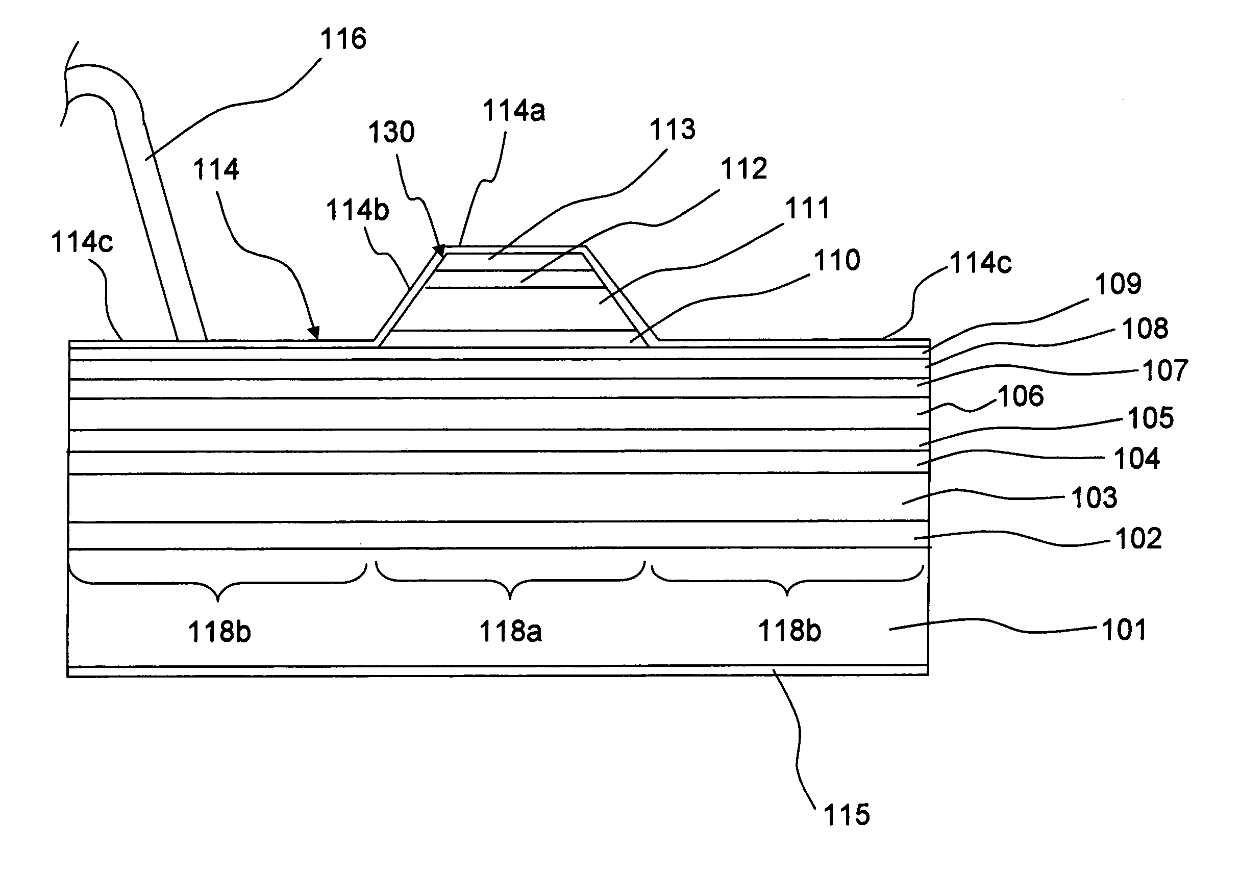
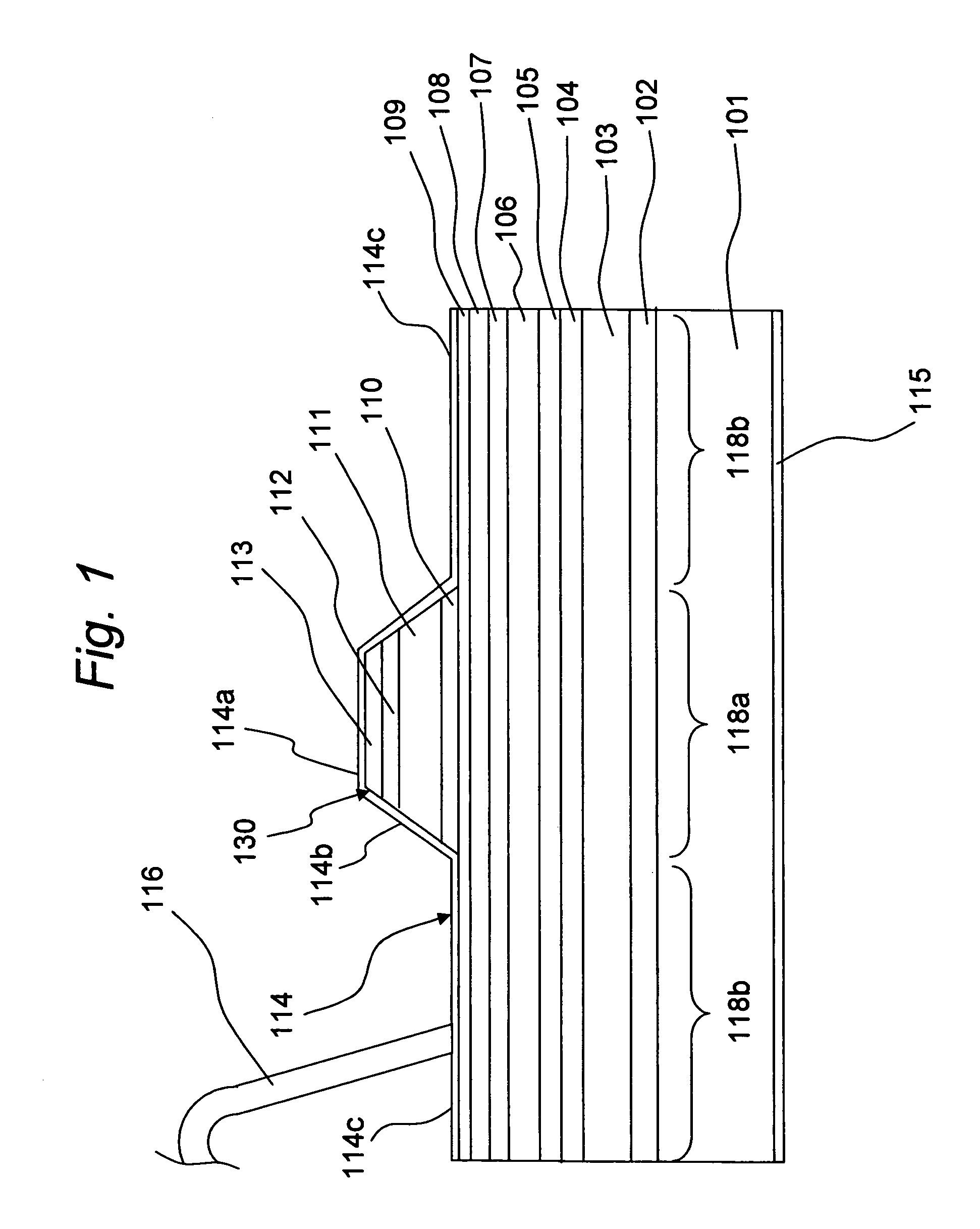
[0137]FIG. 1 shows the structure of a semiconductor laser element for an optical disk (emission wavelength: 780 nm) according to the first embodiment of the present invention.

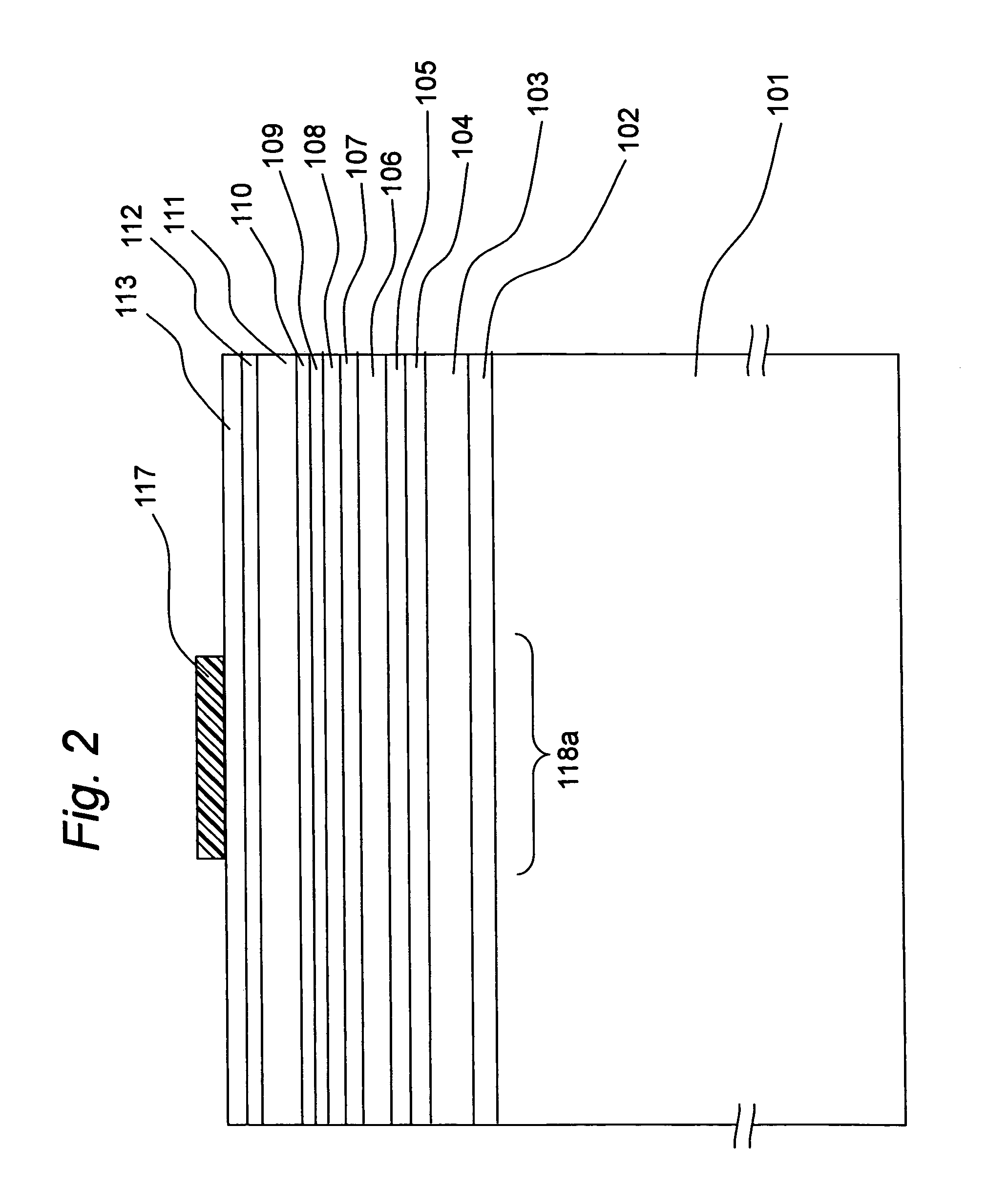
[0138]In this semiconductor laser element, an n-GaAs buffer layer 102, an n-Al0.453Ga0.547As first lower cladding layer 103, an n-Al0.5Ga0.5As second lower cladding layer 104, an Al0.4278Ga0.5722As lower guide layer 105, a multiple strained quantum well active layer 106, an Al0.4278Ga0.5722As upper guide layer 107, a p-Al0.4885Ga0.5115As first upper cladding layer 108 and a p-Al0.4885Ga0.5115As second upper cladding layer 109 are successively stacked in this order on an n-GaAs substrate 101. A p-GaAs etching stopper layer 110, a p-Al0.4885Ga0.5115As third upper cladding layer 111, a p-GaAs contact layer 112 and a p+-GaAs contact layer 113 are provided on the second upper cladding layer 109 so as to form a ridge structure 130 of a forward mesa stripe shape. Further, a p-side electrode 114, which is constructed o...

second embodiment

[0155]FIG. 8 is a schematic sectional view showing the structure of a semiconductor laser element of a second embodiment of the present invention, in which an example obtained by modifying the semiconductor laser element of the first embodiment so as to restrain the absorption by the p-side electrode is shown. In the semiconductor laser element shown in FIG. 8, SiNx films 119 and 119 (thickness: 1500 Å. The SiNx film will be referred to simply as the “SiN film”.) that serve as insulators are provided in a striped manner along both sides of the ridge structure 130 of a forward mesa stripe shape. The SiN films 119 are provided so as to cover side surfaces of the third upper cladding layer 111, side surfaces of the GaAs etching stopper layer 110, and part (3 μm from the ridge structure) of the upper surfaces of the second upper cladding layer 109, and the p-side electrode 114 is provides so as to cover them. That is, each SiN film 119 is provided in a position enclosed by a side surfac...

third embodiment

[0157]FIG. 9 is a schematic sectional view showing the structure of a semiconductor laser element of a third embodiment of the present invention, in which a modification of the semiconductor laser element of the first embodiment is shown. The third embodiment differs from the first embodiment in that stripe-shaped structures 131 are formed on both sides of the ridge structure 130, and is characterized by use of the junction down mounting method in which the laser element is die bonded by using a region on the stripe-shaped structure 131 of the p-side electrode as a bonding surface. The “bonding surface” means a surface of the semiconductor laser chip to be put in contact with a stem or a heat sink on which the semiconductor laser element is mounted.

[0158]The construction and the manufacturing method of the stripe-shaped structures formed on both sides of the ridge structure will be particularly described below, and no detailed description is provided for the constituents common to t...


PUM


Abstract

A semiconductor laser element has a lower cladding layer of first conductivity type, an active layer, a first upper cladding layer of second conductivity type, and a second upper cladding layer of second conductivity type, which are stacked in this order on a semiconductor substrate of first conductivity type. The laser element further has a third upper cladding layer of second conductivity type and a contact layer of second conductivity type, which constitute a stripe-shaped ridge structure. A second-conductivity-type doping concentration of the second upper cladding layer is lower than those of the first and third upper cladding layers and is not higher than 1×1017 cm−3. A sum total of layer thicknesses of the first and second upper cladding layers is 0.3-1.5 μm, inclusive. An electrode layer forms an ohmic junction with the contact layer, and a Schottky junction with the second upper cladding layer.

Description

[0001]This nonprovisional application claims priority under 35 U.S.C. §119(a) on Patent Application Nos. 2003-380688 and 2003-397080 filed in Japan on 11 Nov. 2003 and 27 Nov. 2003, respectively, the entire contents of which are hereby incorporated by reference.BACKGROUND OF THE INVENTION[0002]1. Field of the Invention[0003]The present invention generally relates to semiconductor laser elements and typically to a semiconductor laser element of a high output power and low power consumption for use in an optical disk apparatus, an optical transmission system or the like, and a manufacturing method thereof.[0004]The present invention also relates to an optical disk apparatus and an optical transmission system having such a semiconductor laser element.[0005]2. Description of the Related Art[0006]Among various semiconductor laser elements, a semiconductor laser element of buried ridge structure is able to reduce the parasitic current that does not contribute to laser oscillation and to s...

Claims


Application Information

Patent Timeline
Patent Type & Authority Patents(United States)
IPC IPC(8): H01S3/04H01S5/00H01S5/22H01S5/32H01S5/343
CPCB82Y20/00H01S5/22H01S5/3211H01S5/34353H01S2301/18
Inventor KISHIMOTO, KATSUHIKOKAWANISHI, HIDENORI
Owner SHARP KK
Learn More