
Semiconductor laser diode with low threshold current

A technology of laser diodes and semiconductors, applied in semiconductor lasers, optical waveguide semiconductor structures, lasers, etc., can solve the problems of laser diode threshold current reduction, affecting hole injection, etc.

Inactive Publication Date: 2019-03-05
SHARP KK
View PDF6 Cites 0 Cited by
  • Summary
  • Abstract
  • Description
  • Claims
  • Application Information

AI Technical Summary

Problems solved by technology

This can be achieved by reducing the concentration of dopant species in these layers, however these species can negatively affect hole injection from the p-side semiconductor region and the n-side semiconductor region into the active region
[0020] III-nitride-based semiconductor laser diodes by improving carrier injection and carrier uniformity into the active region while maintaining strong light confinement and high crystallographic quality without degrading the characteristics of the emitted laser light The problem of the threshold current reduction of the

Method used


Image

  • Semiconductor laser diode with low threshold current
  • Semiconductor laser diode with low threshold current
  • Semiconductor laser diode with low threshold current

Examples


Embodiment Construction

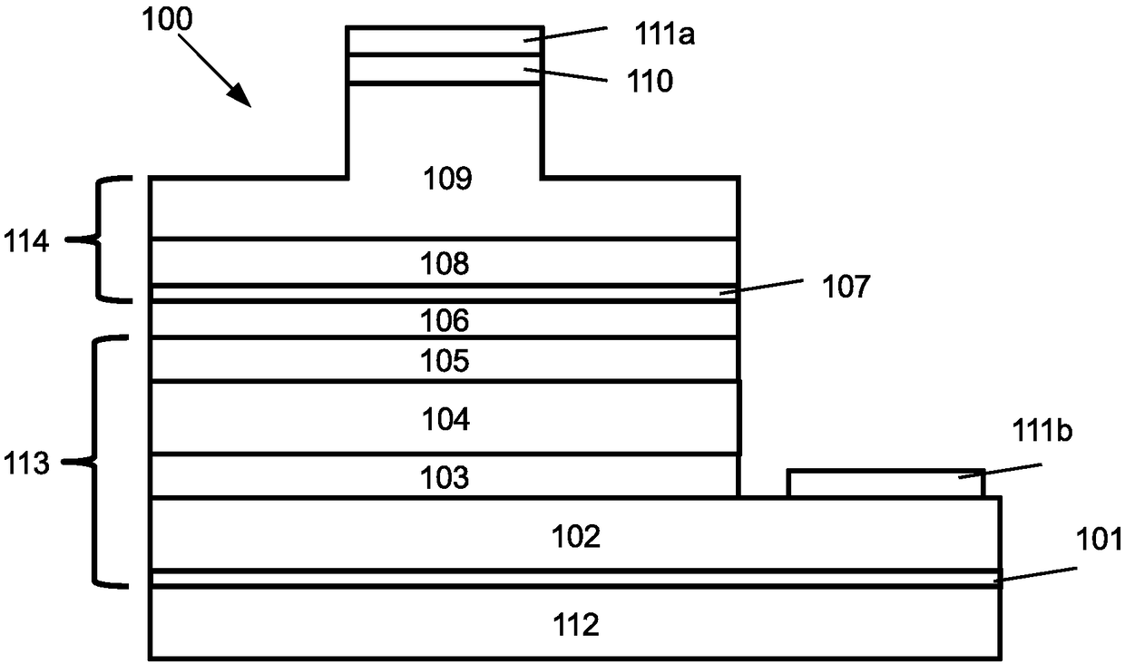
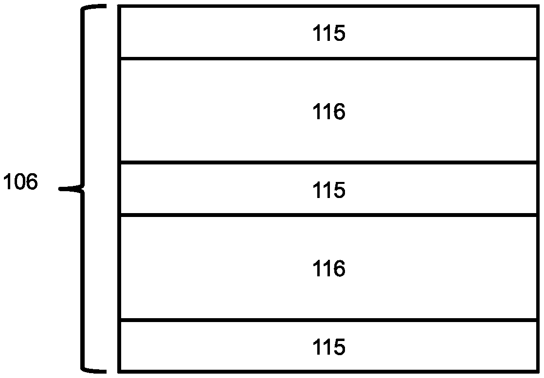
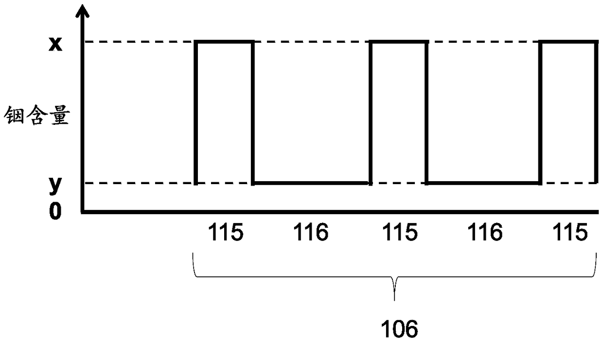
[0058] The present invention provides an active region of a semiconductor laser diode (eg, III-nitride-based laser light emitting diode). The active region may include two quantum well regions, wherein the quantum well closest to the n-side semiconductor has an increased bandgap compared to the quantum well closest to the p-side semiconductor. Devices including multiple quantum well structures for active regions can provide low threshold currents, long lifetimes, and high socket conversion efficiencies.

[0059] now refer to Figure 2A and Figure 2B , 200 illustrates an exemplary embodiment of a semiconductor laser diode (eg, Ill-nitride-based laser light emitting diode) device including an active region. The III-nitride-based laser light-emitting diode device includes an n-side (III-nitride-based) semiconductor region 212, a p-side (III-group nitride-based) semiconductor region 213, and a p-side semiconductor region 213 and n (Ill-nitride based) active region 204 between ...


PUM

PropertyMeasurementUnit
thicknessaaaaaaaaaa
thicknessaaaaaaaaaa
wavelengthaaaaaaaaaa

Abstract

A group III nitride based laser light emitting device includes an n-side group III nitride based semiconductor region, a p-side group III nitride based semiconductor region, and a group III nitride based active region between the p-side group III nitride based semiconductor region and n-side group III nitride based semiconductor region. The group III nitride based active region includes first andsecond quantum well layers and a barrier layer between the first and second quantum well layers, the respective compositions of the first and second quantum well layers comprising different respectiveamounts of indium. The first quantum well is closer to the n-side group III nitride based semiconductor region than the second quantum well, the second quantum well is closer to the p-side group IIInitride based semiconductor region than the first quantum well, and the first quantum well has a larger band gap than the second quantum well.

Description

technical field [0001] The invention relates to the epitaxial structure of semiconductor laser diodes, especially the active region structure of Group III nitride-based semiconductor laser diodes. Background technique [0002] Laser diodes (LDs) based on III-nitride semiconductors are commercially available with emission wavelengths in the UV, blue and green portions of the electromagnetic spectrum. Such devices are used in applications such as lighting and display. It is especially important to provide such devices with high optoelectronic performance. [0003] Group III nitrides (or nitrides) based on GaN and alloys containing In and Al (hereinafter referred to as (Al,In,Ga)N alloys) can be fabricated to form high-efficiency LD devices. The semiconductor layer structure of such devices can be fabricated by sequentially forming semiconductor layers on a substrate. These layers are physically connected and are usually of high crystalline quality obtained by using epitaxia...

Claims


Application Information

Patent Timeline
Patent Type & Authority Applications(China)
IPC IPC(8): H01S5/34H01S5/343
CPCH01S5/3407H01S5/34333H01S5/0014H01S5/2009H01S5/2031H01S5/22H01S5/3211
Inventor 亚力克斯 约丁谷善彦瓦莱里·贝里曼-博斯奎特伊藤茂稔
Owner SHARP KK
Learn More