Semiconductor laser device
a laser device and semiconductor technology, applied in semiconductor lasers, laser details, electrical equipment, etc., can solve the problems of increasing the threshold current of the semiconductor laser device, reducing the optical confinement factor in the active layer, and large width of the near field pattern (nfp) of the laser beam as measured in the crystal growth direction, etc., to achieve high slope efficiency, low threshold current, and high power conversion efficiency
- Summary
- Abstract
- Description
- Claims
- Application Information
AI Technical Summary
Benefits of technology
Problems solved by technology
Method used
Image
Examples
first embodiment
Variations of First Embodiment
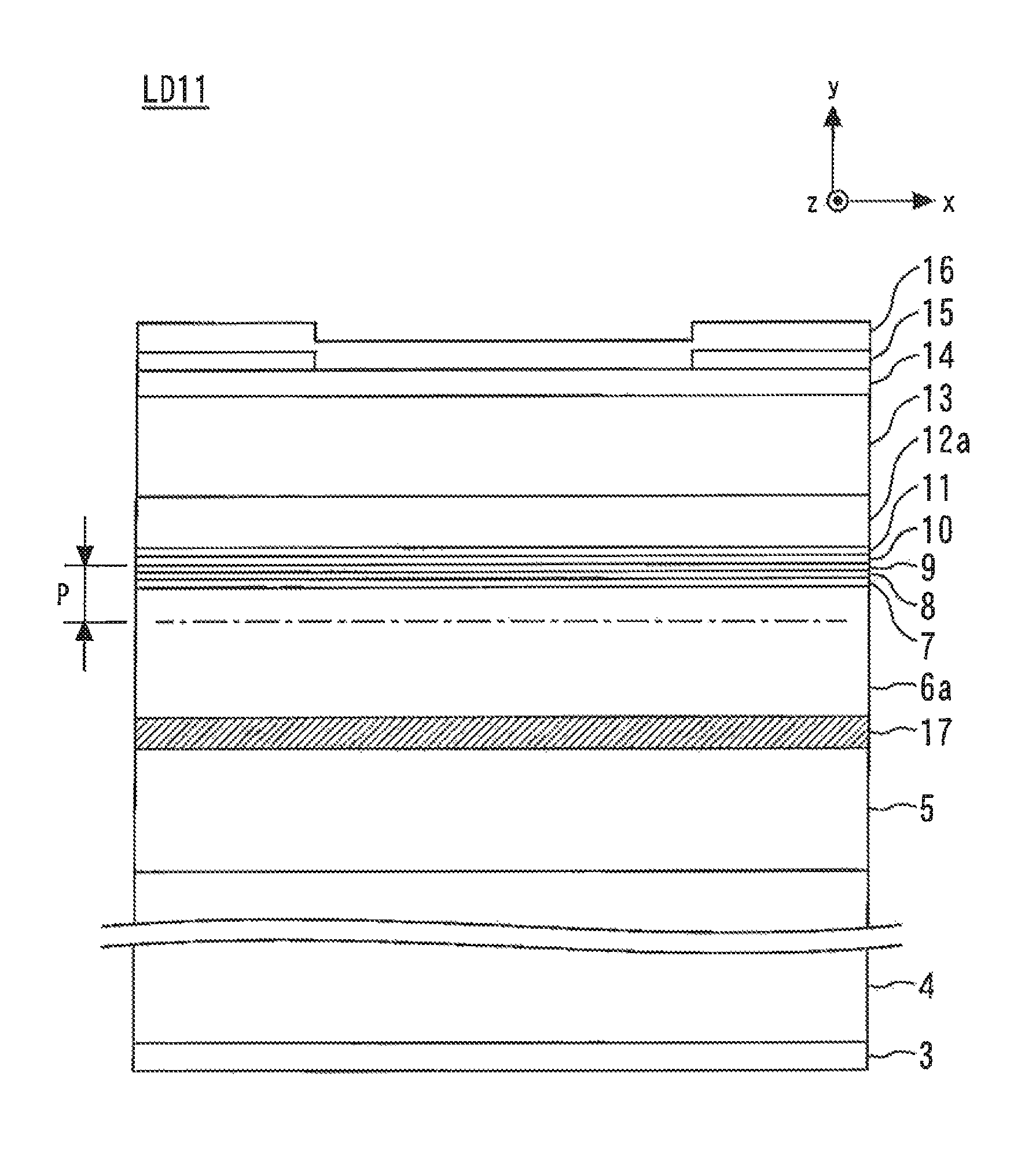
[0092]Although the present embodiment has been described in connection with semiconductor laser devices in which the barrier layers, the light guiding layers, and the cladding layers are made of AlGaAs, it is to be understood that the present invention is not limited to this semiconductor material. The advantages of the present embodiment described above result from a particular relationship between the refractive indices of a plurality of semiconductor layers. Therefore, a semiconductor laser device formed of other material such as GaN-based, AlGaInP-based, or InP-based material may be configured so that the refractive indices of semiconductor layers have the above particular relationship to achieve the advantages of the first embodiment.
[0093]Further, although the semiconductor laser devices of the first embodiment includes an active layer of InGaAs and has a lasing wavelength of 980 nm, it is to be understood that the present invention is not limited...
second embodiment
Configuration of Device of Second Embodiment
[0094]FIG. 9 is a cross-sectional view of a semiconductor laser device LD2 in accordance with a second embodiment of the present invention. This semiconductor laser device is similar in configuration to the semiconductor laser device LD12 of the third practical example of the first embodiment shown in FIG. 6, except that it includes an n-side AlGaAs low refractive index layer 17b instead of the n-side AlGaAs low refractive index layer 17a and further includes a p-side AlGaAs low refractive index layer 18. The n-side AlGaAs low refractive index layer 17b has an Al mole fraction of 0.500 and a thickness of 100 nm. The p-side AlGaAs low refractive index layer 18 has an Al mole fraction x1p and a thickness t1p.
[0095]The semiconductor laser device LD2 of the second embodiment, configured in the manner described above, is characterized by the following two features:
[0096]A first feature is that the p-side AlGaAs low refractive index layer 18, wh...
third embodiment
Configuration of Device of Third Embodiment
[0117]FIG. 12 is a cross-sectional view of a semiconductor laser device LD3 in accordance with a third embodiment of the present invention. The semiconductor laser device LD3 of the third embodiment differs from the semiconductor laser device LD2 of the second embodiment in that the p-side AlGaAs low refractive layer 18 is replaced by a p-side AlGaAs high refractive index layer 19 having a refractive index lower than that of the active layer but higher than that of the p-side AlGaAs light guiding layer 12b. That is, in the semiconductor laser device LD3, the n-side AlGaAs low refractive index layer 17b is provided between the n-type AlGaAs cladding layer 5 and the n-side AlGaAs light guiding layer 6b (as in the second embodiment), and the p-side AlGaAs high refractive index layer 19 is provided between the p-type AlGaAs cladding layer 13 and the p-side AlGaAs light guiding layer 12b.
[0118]The p-side AlGaAs high refractive index layer 19 ha...
PUM
 Abstract
Description
Claims
Application Information
 - R&D
- Intellectual Property
- Life Sciences
- Materials
- Tech Scout
- Unparalleled Data Quality
- Higher Quality Content
- 60% Fewer Hallucinations
Browse by: Latest US Patents, China's latest patents, Technical Efficacy Thesaurus, Application Domain, Technology Topic, Popular Technical Reports.
© 2025 PatSnap. All rights reserved.Legal|Privacy policy|Modern Slavery Act Transparency Statement|Sitemap|About US| Contact US: help@patsnap.com


