
High-voltage generating circuit including charge transfer switching circuit for selectively controlling body bias voltage of charge transfer device

a high-voltage generating circuit and switching circuit technology, applied in electronic switching, digital storage, instruments, etc., can solve the problems of significant reduction of charge transfer efficiency, and achieve the effect of increasing the efficiency of charge transfer during charge transfer, reducing and/or preventing a backflow of charges

Active Publication Date: 2009-02-17
SAMSUNG ELECTRONICS CO LTD
View PDF14 Cites 0 Cited by
  • Summary
  • Abstract
  • Description
  • Claims
  • Application Information

AI Technical Summary

Benefits of technology

[0026]Accordingly, a boosted voltage generating circuit according to example embodiments is capable of selectively controlling a bulk voltage of a transistor in a charge transfer switch circuit in order to increase the efficiency of charge transfer during charge transfer, and reducing and / or preventing a backflow of charges during precharging.

Problems solved by technology

Further, if VPP is low, the gate voltage of the NMOS transistor is lowered, thereby significantly reducing the efficiency of charge transfer.

Method used


Image

  • High-voltage generating circuit including charge transfer switching circuit for selectively controlling body bias voltage of charge transfer device
  • High-voltage generating circuit including charge transfer switching circuit for selectively controlling body bias voltage of charge transfer device
  • High-voltage generating circuit including charge transfer switching circuit for selectively controlling body bias voltage of charge transfer device

Examples


Embodiment Construction

[0034]Various example embodiments will now be described more fully with reference to the accompanying drawings. However, specific structural and functional details disclosed herein are merely representative for purposes of describing example embodiments, and one skilled in the art will appreciate that example embodiments may be embodied in many alternate forms and should not be construed as limited to only the embodiments set forth herein.

[0035]It should be understood that, although the terms first, second, etc. may be used herein to describe various elements, these elements should not be limited by these terms. These terms are only used to distinguish one element from another. For example, a first element could be termed a second element, and, similarly, a second element could be termed a first element, without departing from the scope of the example embodiments. As used herein, the term “and / or” includes any and all combinations of one or more of the associated listed items.

[0036]...


PUM


Abstract

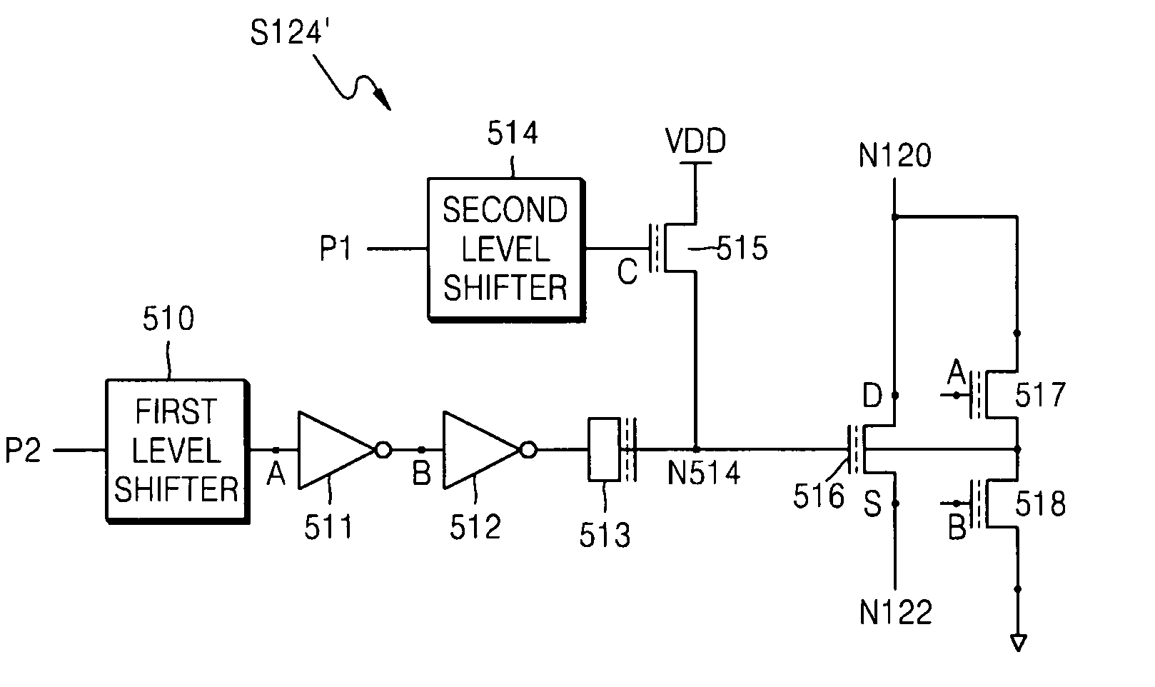
Provided are a charge transfer switch circuit for selectively controlling body bias voltage of a charge transfer device, and a boosted voltage generating circuit having the same. The charge transfer switch circuit may include a capacitor whose voltage is boosted based on first and second control signals, a first transistor connected between a supply voltage and the capacitor and having a gate receiving a precharge signal, a second transistor connected between a first node and a second node and having a gate connected to a terminal of the capacitor, a third transistor connected between the first node and a bulk voltage of the second transistor and having a gate receiving the first control signal, and a fourth transistor connected between the bulk voltage of the second transistor and a ground voltage and having a gate receiving the second control signal.

Description

PRIORITY STATEMENT[0001]This application claims the benefit of priority from Korean Patent Application No. 10-2006-0017883, filed on Feb. 23, 2006 in the Korean Intellectual Property Office, the entire contents of which is incorporated herein by reference.BACKGROUND[0002]1. Field[0003]Example embodiments relate to a semiconductor integrated circuit. More particularly, example embodiments relate to an electric charge transfer switch circuit for selectively controlling a body bias voltage of a charge transfer device and a boosted voltage generating circuit having the same.[0004]2. Description of the Related Art[0005]Recently, DRAMs have been developed that are directed towards increasing the integration degree of memory cells of DRAMS while reducing the size of each memory cell and lowering an external supply voltage for the DRAM. For example, a supply voltage VDD for a DRAM may be lowered from approximately 5V to approximately 1.8V or 1.5V. If the supply voltage VDD is lowered to app...

Claims


Application Information

Patent Timeline
Patent Type & Authority Patents(United States)
IPC IPC(8): G05F1/10
CPCG11C5/145G11C11/4074G11C5/147G11C11/4072
Inventor KIM, JUNG-SIKHWANG, SOO-MANJANG, YOUNG-MIN
Owner SAMSUNG ELECTRONICS CO LTD
Learn More