
Method of Manufacturing a Solid Image Pick-Up Device and a Solid Image Pick-Up Device

a pickup device and solid image technology, applied in the direction of color television, television system, radio control device, etc., can solve the problems of shading, scattering of sensitivity, worsening of smear by stray light, and significant problems, and achieve the effect of high accuracy and easy formation

Inactive Publication Date: 2008-10-02
FUJIFILM CORP
View PDF21 Cites 5 Cited by
  • Summary
  • Abstract
  • Description
  • Claims
  • Application Information

AI Technical Summary

Benefits of technology

The invention provides a method for manufacturing a solid image pick-up device with improved charge transfer efficiency. The method includes steps of forming a pattern of a first layer conductive film, removing a second layer conductive film over the first layer conductive film to planarize the surface, adding a dummy pattern to prevent film reduction, and coating a resist over the second layer conductive film. The method also includes steps of etching the dummy pattern and forming a trench to surround the effective image pick-up region. The invention aims to prevent short circuits and improve the surface level of the resist, resulting in a highly reliable solid image pick-up device.

Problems solved by technology

Accordingly, a positional accuracy between the lens and the photoelectronic conversion portion is important, and the distance, that is, the distance in the direction of the height thereof provides a significant problem in view of the positional accuracy in manufacturing steps and in view of the sensitivity during use (photoelectronic conversion efficiency).
This results in a problem of scattering for the interconnection resistance in such a case.
In the case as described above, there was a problem of scattering for the interconnection resistance at the periphery.
Then, this results in unevenness for the thickness and the variation of the shape in various kinds of films such as a planarized film, micro lens, color filter, etc. above the charge transfer electrode and they also result in a problem of shading, scattering of sensitivity and worsening of smear by stray light.
Accordingly, the method described above involves a problem that it is difficult to cope with the further improvement of the sensitivity.
As described above, existent solid image pick-up devices involve a problem that the thickness of the doped second layer amorphous silicon film is decreased in a region of the first electrode constituting the first layer over the semiconductor substrate where the pattern density is small, particularly, in the circumferential periphery of the wafer.

Method used


Image

  • Method of Manufacturing a Solid Image Pick-Up Device and a Solid Image Pick-Up Device
  • Method of Manufacturing a Solid Image Pick-Up Device and a Solid Image Pick-Up Device
  • Method of Manufacturing a Solid Image Pick-Up Device and a Solid Image Pick-Up Device

Examples


first embodiment

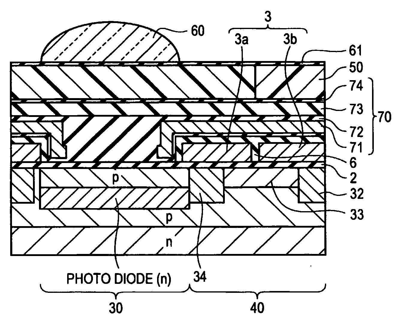
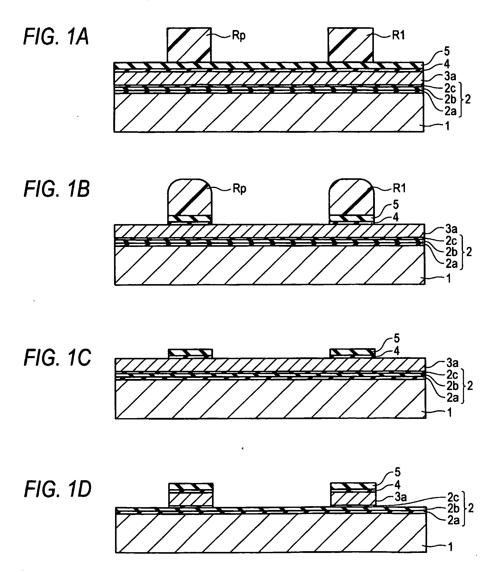
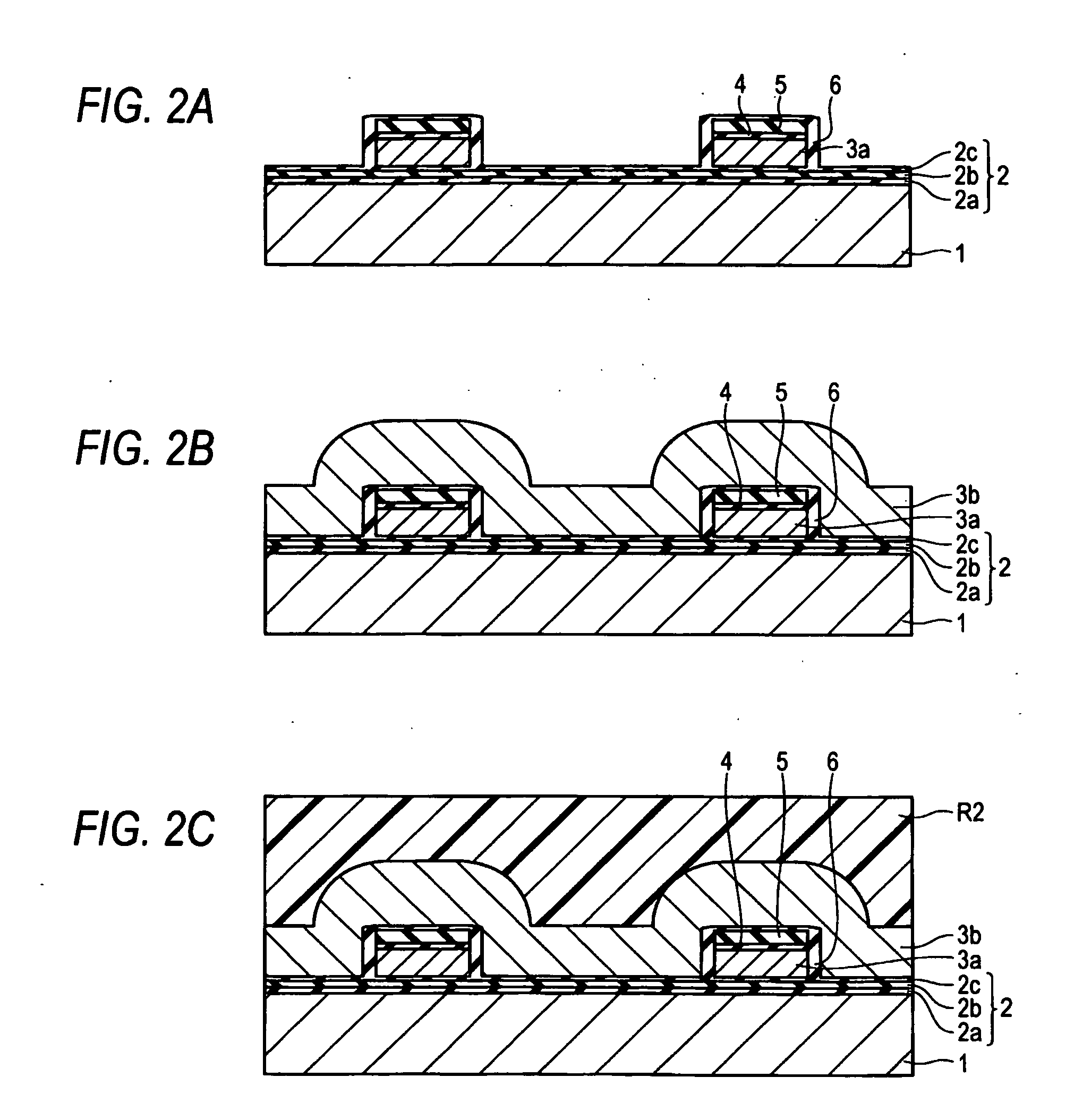
[0064]The solid image pick-up device has a feature, as shown by an electrode forming step in FIGS. 1A to 1D to FIGS. 3A and 3B, has a constitution in that a pattern of a first layer amorphous silicon film constituting a first electrode has a dummy pattern at the periphery of a semiconductor substrate upon forming a solid image pick-up device having a charge transfer electrode of a single layered electrode structure, and the pattern distance is not larger at the periphery of the semiconductor substrate than the inter-electrode distance of the first electrode.

[0065]Thus, film reduction is not caused to the periphery also for the second electrode and the interconnection constituted with a second layer amorphous silicon by planarization by resist etching-back. Accordingly, in the charge transfer portion and the peripheral circuit portion, surface can be planarized satisfactorily with no film reduction.

[0066]As shown in FIG. 4 and FIG. 5 for the entire outlined explanatory view (peripher...

second embodiment

[0094]While the dummy pattern has been left and used as the ground line in the first embodiment, it may be removed after the resist etching-back treatment.

[0095]That is, the second embodiment is different from the first embodiment in that the resist pattern R3 for forming the peripheral circuit shown in FIG. 3B is constituted with a resist pattern R3′ not containing the dummy pattern.

[0096]As shown in FIG. 7A, a resist pattern R3′ covering the peripheral circuit forming portion and the charge transfer portion are formed to the surface of the substrate planarized by etching-back. As apparent form the comparison with FIG. 3B, this embodiment is different only in that the resist pattern R3′ not containing the dummy pattern is used.

[0097]In this case, the resist pattern R3′ is formed so as to cover the solid image pick-up device forming portion and a portion of the peripheral circuit portion and expose the dummy pattern.

[0098]Then, as shown in FIG. 7B, the doped second layer amorphous s...

third embodiment

[0103]Also not described specifically in the embodiment described above, a field oxide film is formed in a frame-like shape at the chip peripheral portion so as to surround the effective image pick-up region thereof and it is preferably formed by a recess LOCOS method such that the surface level is identical between the photoelectronic conversion portion having a photosensor and the charge transfer portion.

[0104]In the solid image pick-up device of this embodiment, the surface level of the field oxide film disposed to the peripheral circuit portion and the charge transfer portion is made about at the identical surface level with that of the photoelectronic conversion portion, and the entire substrate surface is planarized upon formation of the device region thereby improving the pattern accuracy by photolithography, by which the film reduction of the conductive film, particularly, the second layer conductive film caused upon making the charge transfer electrode into a single layered...


PUM


Abstract

A method of manufacturing a solid image pick-up device comprising a photoelectronic conversion portion, a charge transfer portion and a peripheral circuit portion, the method comprising:forming a pattern comprising a first layer silicon conductive film to a surface of a semiconductor, the first layer silicon conductive film forming: a first electrode; and a first layer interconnection for the photoconductive conversion portion and the peripheral circuit portion; forming an insulative film at least to a side wall of the first electrode; forming a second silicon conductive film being to form a second electrode to the semiconductor substrate; coating a resist over the semiconductor substrate by a spin coating method; and planarizing the second layer silicon conductive film by a resist etching-back method,wherein the pattern further comprises at least one dummy pattern, and a surface level of the resist is not below a predetermined value over the semiconductor substrate.

Description

TECHNICAL FIELD[0001]The present invention concerns a method of manufacturing a solid image pick-up device, and a solid image pick-up device and, particularly, it relates to a solid image pick-up device of a single layered electrode CCD (charge-coupled device) structure.BACKGROUND ART[0002]A solid image pick-up device using a CCD used, for example, in an area sensor comprises a photoelectronic conversion portion such as a photodiode and a charge transfer portion having a charge transfer electrode for transferring signal charges from the photoelectronic conversion portion. Charge transfer electrodes are arranged in plurality adjacent with each other on a charge transfer channel formed to a semiconductor substrate and driven successively.[0003]In recent years, a demand for higher resolution and higher sensitivity for solid image pick-up devices has been increased more and more and increase for the number of image pick-up pixels has been proceed as far as giga pixels or more. A substra...

Claims


Application Information

Patent Timeline
Patent Type & Authority Applications(United States)
IPC IPC(8): H01L27/148H01L21/768H01L27/146H04N25/00
CPCH01L27/14687H01L27/14812H01L27/14843H01L29/66954H01L29/76866H01L27/146
Inventor AZUMI, TEIJISATO, TAKANORI
Owner FUJIFILM CORP
Learn More