
Multi-band RF transceiver with passive reuse in organic substrates

a multi-band, organic substrate technology, applied in the field of passive components, can solve the problems of power consumption, compatibility, interference, integration, and the need for additional design components to support such multi-band, multi-mode capabilities, and power consumption challenges

Active Publication Date: 2009-02-10
GEORGIA TECH RES CORP
View PDF103 Cites 43 Cited by
  • Summary
  • Abstract
  • Description
  • Claims
  • Application Information

AI Technical Summary

Benefits of technology

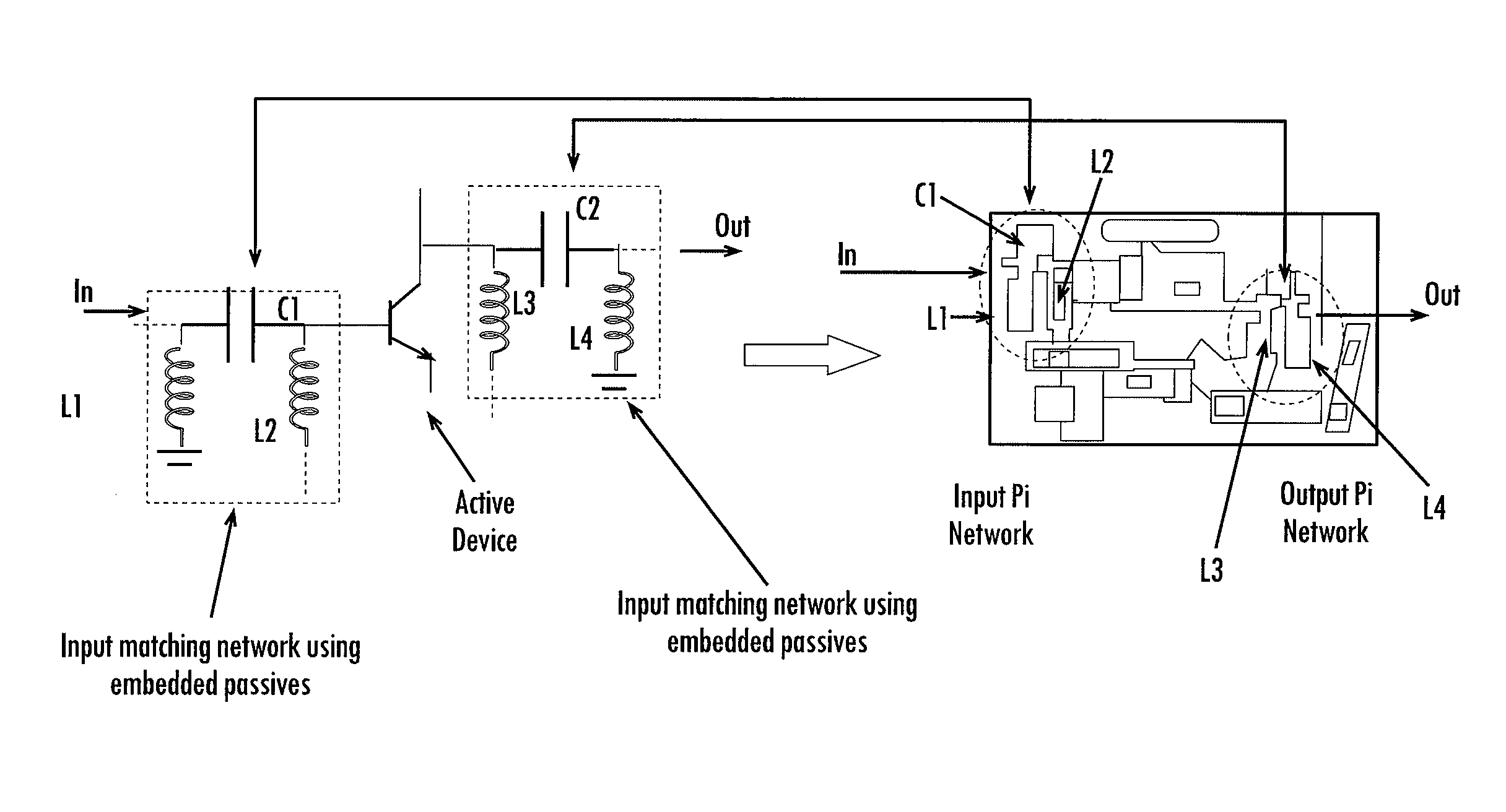
The present invention describes a new approach to designing RF transceivers that can work at multiple frequency ranges using a single chip. This is achieved by using high-Q passives embedded in organic substrates, which can be reused at different frequencies. The invention also includes voltage controlled oscillators and low noise amplifiers with low phase noise. The invention also describes a multi-band RF device that can simultaneously generate oscillation signals at different frequencies using a feedback network. Additionally, the invention includes a multi-band low noise amplifier that can have desired power gains at different frequencies by using matching networks with different reactance at different frequencies. Overall, the invention reduces the number of components required and improves the performance of RF transceivers.

Problems solved by technology

Designing multi-band, multi-mode devices such as RF transceivers presents some difficulties in power consumption, compatibility, interference, and integration.
For example, the need for the additional design components to support such multi-band, multi-mode capabilities oftentimes presents challenges with power consumption.
This may be especially problematic in a portable multi-band, multi-mode device such as a cell phone operating on a battery.
The battery life of the cell phone would decrease as the power consumption requirements of the components within the cell phone increase.
Further, as many devices continue to decrease in size, the inclusion of additional components becomes increasingly difficult due to problems such as routing, interference, etc.
Achieving the required quality factors (Qs) of these components may become more difficult with these size constraints.

Method used


Image

  • Multi-band RF transceiver with passive reuse in organic substrates
  • Multi-band RF transceiver with passive reuse in organic substrates
  • Multi-band RF transceiver with passive reuse in organic substrates

Examples


example i

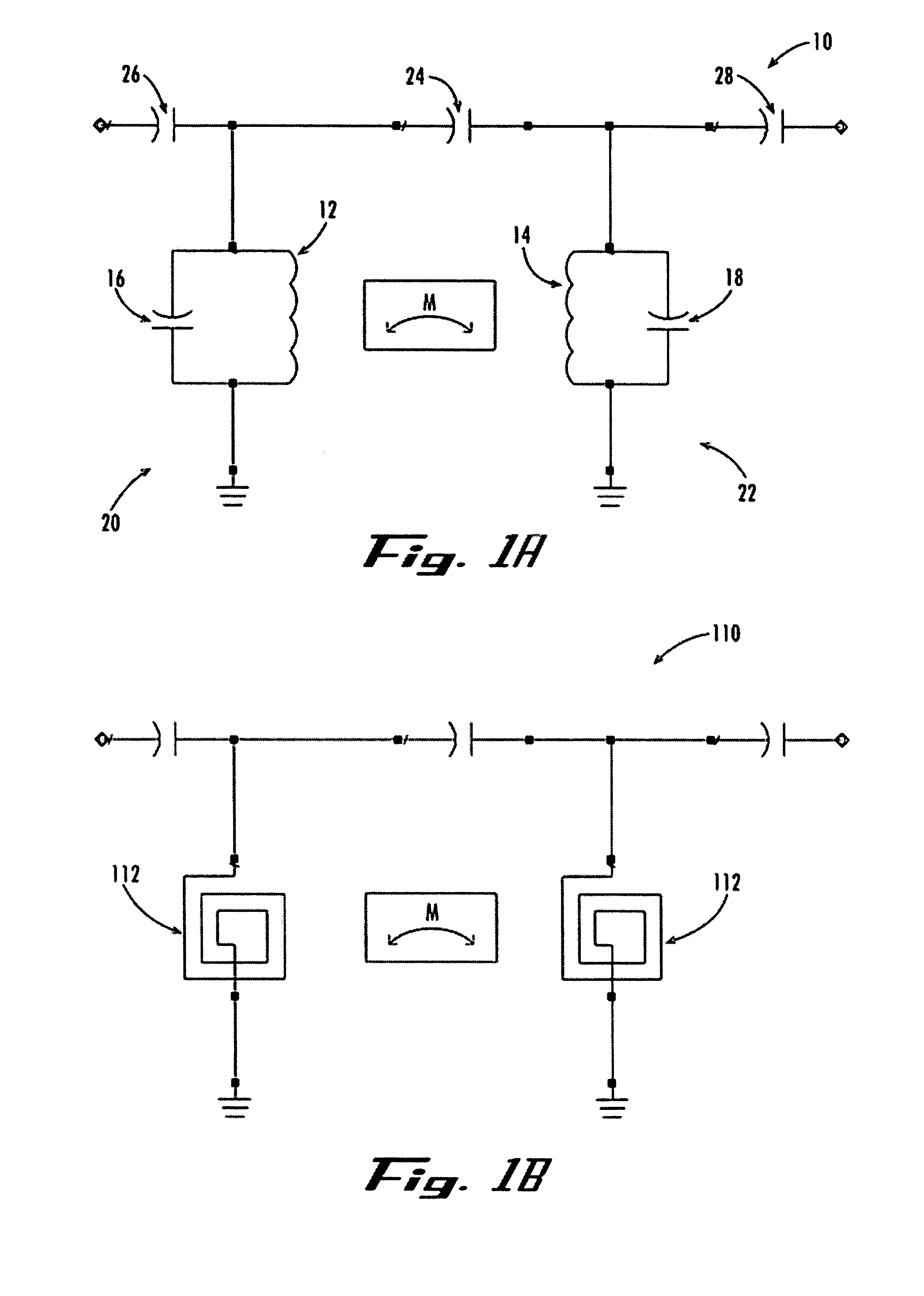
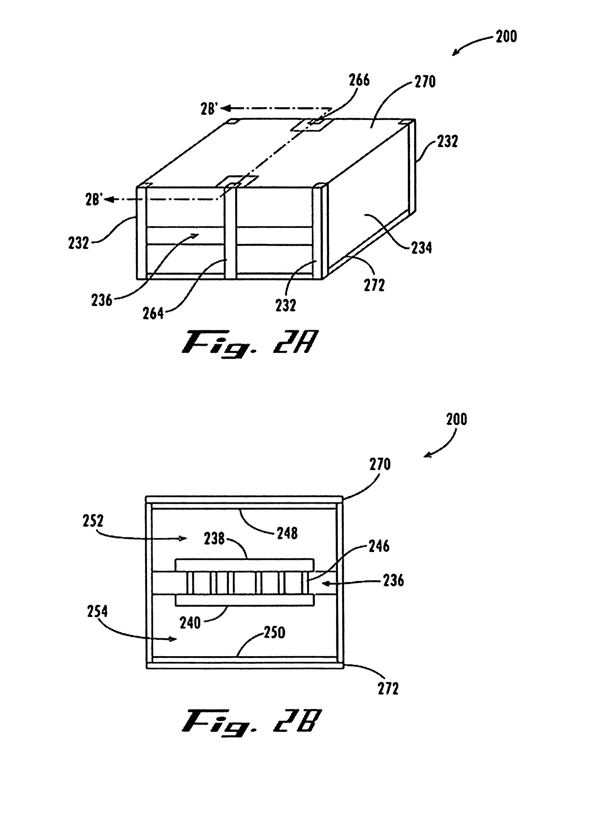
[0092]An X-ray photograph of an organic bandpass filter 500 in accordance with an embodiment of the present invention is provided in FIGS. 7 and 8. The filter 500 comprises shorted hybrid CPW-stripline meander transmission line inductors 512, 514 formed close to each other on a first organic dielectric layer, which is a 50 μm thick layer of LCP, wherein the inductors 512, 514 are directly magnetically coupled to each other. Each inductor is connected to separate parallel plate capacitors 516, 518 by sandwiching the same dielectric sheet. An inter-resonator parallel plate coupling capacitor 524, is formed using two disconnected metal plates that sandwich the same organic dielectric sheet in such a manner that the each plate of the inter-resonator coupling capacitor electrode connects to separate inductors. In addition, a second organic dielectric layer and a third organic dielectric layer sandwich the first organic dielectric layer, and comprise a high frequency hydrocarbon material ...

example ii

[0103]Another organic bandpass filter 600 in accordance with an embodiment of the present invention is shown in the picture of FIG. 10. The filter 600 comprises shorted hybrid CPW-microstrip, meander inductors 612, 614 formed close to each other on a first organic dielectric layer, which is a layer of LCP, directly magnetically coupled to each other. The term “shorted” refers to one end of each inductor connected to the large metallic area, which in this case serves as the in-built shield 630 (also referred to as a coplanar ground ring). In addition, the filter 600 includes an inter-resonator parallel plate coupling capacitor electrode 624 with in-built shield 630 formed using two disconnected metal plates that sandwich the first organic dielectric layer in such a manner that the each plate of the inter-resonator coupling capacitor electrode connects to separate resonators. Yet further, the filter 600 includes a first shield electrode formed respectively on a second organic dielectr...

example iii

[0112]Yet another organic bandpass filter 700 in accordance with an embodiment of the present invention is shown in the picture of FIG. 12. The organic bandpass filter 700 comprises shorted hybrid CPW-microstrip meander inductors formed close to each other on a first organic dielectric substrate, such as epoxy based Vialux by E.I. du Pont de Nemours and Company, directly magnetically coupled to each other. In addition, the third bandpass filter comprises an inter-resonator parallel plate coupling capacitor electrode 724, with ground ring, formed using two disconnected metal plates that sandwich the same organic dielectric sheet in such a manner that the each plate of the inter-resonator coupling capacitor electrode connects to separate resonators.

[0113]The transmission line inductors 712, 714 did not provide the needed capacitance in the desired length. Since the dielectric is lossy for the capacitor application, each is replaced by a separate discrete capacitor 702, such as a chip ...


PUM


Abstract

The present invention allows for the use of chip-package co-design of RF transceivers and their components by using discrete active devices in conjunction with passive components. Two particular components are described, including voltage controlled oscillators (VCOs) and low noise amplifiers (LNAs). The high quality passive components for use in the VCOs and LNAs may be obtained by the use of embedded passives in organic substrates. Further, the embedded passives may have multi-band characteristics, thereby allowing multi-band VCOs and LNAs to be implemented with fewer components. In situations where size is a concern, the active devices and passive components utilized in an RF transceiver may be implemented in a low form factor module of less than 1.1 mm thick according to an embodiment of the invention.

Description

CROSS-REFERENCE TO RELATED APPLICATIONS[0001]This application claims benefit of U.S. Provisional Application No. 60 / 565,254, filed Apr. 23, 2004, entitled “Digitally Tunable Compact Multiband Low Noise Amplifiers Through Passive Re-use.” This application is also a continuation-in-part of U.S. patent application Ser. No. 10 / 402,313, filed Mar. 28, 2003, now U.S. Pat. No. 6,900,708 entitled “Integrated Passive Devices Fabricated Utilizing Multi-Layer, Organic Laminates.” All of the foregoing applications are incorporated herein by reference.BACKGROUND OF THE INVENTION[0002]I. Field of the Invention[0003]The present invention generally relates to passive components, and more particularly to the chip-package co-design of RF single-band and multi-band transceivers using high quality embedded passive components in organic substrates for use in radio frequency (RF) applications.[0004]II. Description of Related Art[0005]With a proliferation of wireless standards and applications operating a...

Claims


Application Information

Patent Timeline
Patent Type & Authority Patents(United States)
IPC IPC(8): H04B1/18H01P1/203H03B1/00H03B5/12H03H7/09H03H7/38H03H7/46H03H11/00H05K1/02H05K1/16H05K3/46
CPCH01P1/20381H03F3/195H03H7/09H03H7/1775H03H7/38H03H7/46H03B5/1228H03B5/1231H03B5/1215H03B5/1203H03F2200/111H03H2001/0085H05K1/024H05K1/16H05K3/4623H05K3/4626H01L2224/16227H01L2224/48091H01L2224/48227H01L2924/19105
Inventor GOVIND, VINUDALMIA, SIDHARTHBAVISI, AMITSUNDRARAM, VENKATESHSWAMINATHAN, MADHAVANWHITE, GEORGE
Owner GEORGIA TECH RES CORP
Learn More