
Method for manufacturing selective area grown stacked-layer electro-absorption modulated laser structure

a laser structure and selective area technology, applied in semiconductor lasers, instruments, optics, etc., to achieve excellent device characteristics

Active Publication Date: 2009-01-13
INST OF SEMICONDUCTORS - CHINESE ACAD OF SCI
View PDF16 Cites 14 Cited by
  • Summary
  • Abstract
  • Description
  • Claims
  • Application Information

AI Technical Summary

Benefits of technology

[0012]An object of the present invention is to provide a method for manufacturing a selective area grown stacked-layer electro-absorption modulated laser structure, which can obviously improve the characteristics of EML integrated devices, has the advantages of low threshold current, high extinction ratio and high optical output power, and can grow a stacked-layer structure of an LD active layer and an EAM active layer only by one epitaxy, and the process is simple, which is suitable for large-scale mass production.
[0029]The present invention makes full use of the features of the SAG technology and the improved stacked-layer technology, and not only remains the advantages of these two technologies, but also greatly weakens the disadvantages thereof, so it is possible for these two technologies to reinforce each other to realize excellent characteristics of devices which is impossible only by either of these two.

Problems solved by technology

However, the Butt-Joint method requires multiple epitaxial growths, complex manufacturing process and very high precision requirements of the process.
Additionally, the joining interface of the active sections, that is the joining interface of the EAM active section and the LD active section, which are respectively grown by two epitaxies, usually leads to crystal quality problems such as holes or bumps, causing the low yield and high cost of EMLs.
1) Selective area growth (SAG) method. The EML devices manufactured by the famous corporations, such as NTT, Fujitsu, Nortel and Siemens, adopt the SAG method. This method grows multiple quantum well (MQW) active layers by one epitaxy (for example, Chinese Patent No. ZL00109780.6), and can get the bandgap wavelength difference between LD-MQW active layer and EAM-MQW active layer up to 30 meV. Although the SAG method greatly simplifies the growth process and reduces the cost, its brought problem is that the structure parameters of the LD-MQW active layer and those of the EAM-MQW active layer constrain each other, which is difficult to deal with in a single epitaxy. For example, in terms of reducing the threshold current and weakening the influence of non-uniform carrier implantation, the number of the QW in the LD active layer is required to be small and the thickness of the wells is required to be thin, but in terms of extinction ratio, the number of the QW in the EAM active layer is required to be large and the thickness of the wells is required to be thick. When the EML is actually manufactured by the SAG method, the numbers of the wells in the two active layers are equal, which is the tradeoff between the two sections, but it can not overcome the disadvantage that the thickness of the wells in the LD active layer is thick while the thickness of the wells in the EAM active layer is thin. Therefore, compared with the Butt-Joint method, the optical output power and the extinction ratio of the EML devices manufactured by the SAG method is inferior, and it's difficult to improve the characteristics of the devices.
2) Identical active layer (IAL) method, for example, U.S. Pat. No. 5,548,607. The manufacturing process of this method is simplest, because the active layer structures of the LD and the EAM are identical. The wavelength difference between LD section and EAM section is implemented by the red-shift of the oscillating wavelength determined by the Bragg gratings etched in the LD region relative to the peak wavelength of the QW active layer. However, the EAM section strongly absorbs the light from the LD region after all, so the threshold current of the device is high. It is difficult to improve the whole characteristics of EMLs by the IAL method.
3) QW intermixing (QWI) method, for example, IEEE Photonics Technology Letters, Vol. 7(9), P. On the basis of the IAL structure, this method makes intermixing of the MQW in the EAM section by ion implantation or dielectric induced diffusion plus annealing and so on to cause the blue-shift of the absorption peak wavelength of the MQW in this region, so as to reduce the absorption loss and improve the characteristics. However, till now, the repeatability of the intermixing technology hasn't be solved effectively.
4) Stacked-layer MQW structure, for example, IEEE Photonics Technology Letters, Vol. 14(12), P. This method grows the 2-stacked-layer MQW structure by one epitaxy, one layer EAM-MQW and another layer LD-MQW, and the two layers can be designed respectively so that the bandgap wavelength difference between them is no more than 60 nm. However, the EAM-MQW layer in the LD section not only absorbs the light from the LD-MQW, but also consumes the injection carrier, and the LD-MQW layer in the EAM section has relatively strong absorption of light when there is no bias voltage, so EML devices of stacked-layer MQW structure have high threshold current and low optical output power. In 2003, we proposed an improved stacked-layer MQW structure (Chinese patent application No. 200310122343.7), which improves the optical output power significantly by etching the LD-MQW layer in the EAM section away by photolithography and selective etching. However, the problem of high threshold current of these EMLs hasn't been solved yet.

Method used


Image

  • Method for manufacturing selective area grown stacked-layer electro-absorption modulated laser structure
  • Method for manufacturing selective area grown stacked-layer electro-absorption modulated laser structure
  • Method for manufacturing selective area grown stacked-layer electro-absorption modulated laser structure

Examples


Embodiment Construction

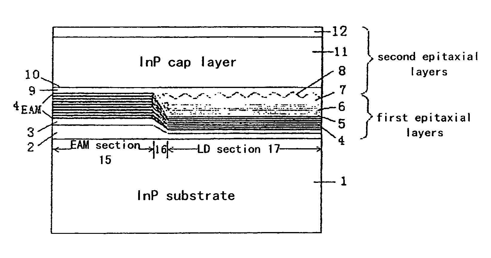
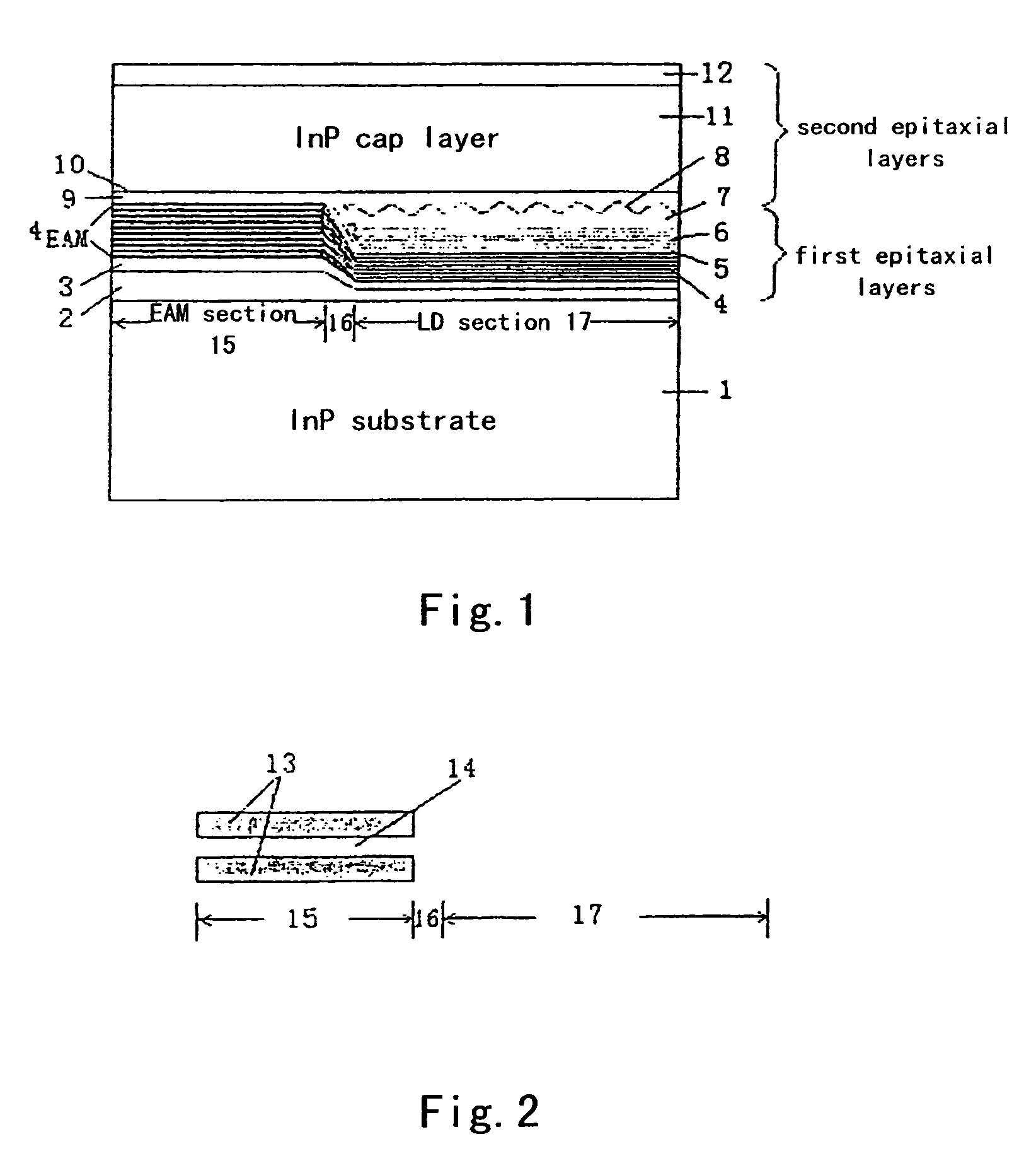
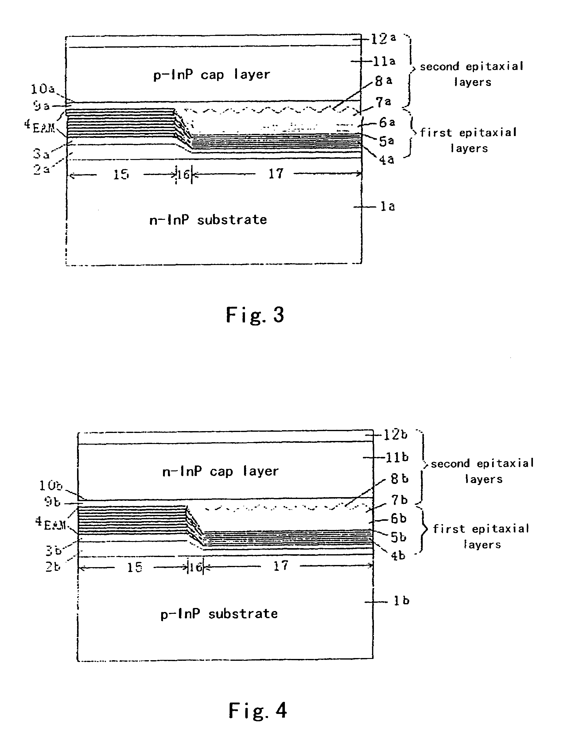
[0035]Referring to FIG. 1 and FIG. 2, a method for manufacturing a selective area grown stacked-layer electro-absorption modulated laser structure comprises following steps.

[0036]Step 1: a selective growth pattern of a modulator section 15 is formed on a substrate 1, wherein the selective growth pattern of the modulator 15 is two dielectric film stripes 13, which have a length of 100-300 μm and a width of 10-50 μm, an opening width 14 of the selective growth between the two dielectric stripes is 10-40 μm; wherein said dielectric film is of SiO2 or Si3N4, and has a thickness of 100-300 nm; wherein a length of the modulator section 15 is 100-300 μm, a length of a laser section 17 is 200-600 μm, and a transition region 16 between the modulator section 15 and the laser section 17 has a length of 30-100 μm, and the transition region 16 is also of a length of the electrically isolating section between the modulator and the laser;

[0037]Step 2: a 2-stacked-layer active region structure of a...


PUM


Abstract

This invention relates to a method for manufacturing selective area grown stacked-layer electro-absorption modulated laser structure, comprising: step 1: forming a selective growth pattern of a modulator section on a substrate; step 2: simultaneously growing a 2-stacked-layer active region structure of a modulator MQW layer and a laser MQW layer by the first epitaxy step; step 3: etching gratings, and removing the laser MQW layer in the modulator section by selective etching; and step 4: completing the growth of the entire electro-absorption modulated laser structure by a second epitaxy step.

Description

[0001]This application claims priority from Chinese Application No. 2004100778635, filed Sep. 16, 2004 (incorporated by reference Herein) and Chinese Application No. 2005100045713, filed Jan. 18, 2005 (incorporated by reference herein).BACKGROUND OF THE INVENTION[0002]1. Field of Invention[0003]The present invention relates to semiconductor technologies, and more particularly, to a method for manufacturing a selective area grown (SAG) stacked-layer electro-absorption modulated distributed feedback lasers (EMLs) structure, which has the advantage of simple process and fabricates monolithically integrated EML of low threshold current.[0004]2. Description of Prior Art[0005]A monolithically integrated device of an electro-absorption modulator (EAM) and a distributed feedback (DFB) laser diode (LD), EML, is a significant transmitting light-source of optical communication systems, especially, in high speed long-haul trunks. At present, a main method for manufacturing the EML integrated li...

Claims


Application Information

Patent Timeline
Patent Type & Authority Patents(United States)
IPC IPC(8): H01L21/00H01S5/12
CPCB82Y20/00G02F1/01708H01S5/0265H01S5/1039H01S5/12H01S2304/00
Inventor ZHU, HONGLIANGWANG, WEI
Owner INST OF SEMICONDUCTORS - CHINESE ACAD OF SCI
Learn More