Method for reducing device and circuit sensitivity to electrical stress and radiation induced aging

a technology of electrical stress and radiation induced aging, applied in the direction of basic electric elements, semiconductor/solid-state device manufacturing, electric devices, etc., can solve the problems of h or h, deleterious effect etc., to achieve positive bias temperature instability, increase the temperature of device operation, and increase the power consumption

Inactive Publication Date: 2008-12-02
THE GOVERNMENT OF THE UNITED STATES AS REPSESENTED BY THE SEC OF THE AIR FORCE
View PDF4 Cites 1 Cited by
  • Summary
  • Abstract
  • Description
  • Claims
  • Application Information

AI Technical Summary

Benefits of technology

[0009]The escaping hydrogenous species diffuses away either through the dielectric film or into the semiconductor. In the former case, two H↑ species will ultimately encounter and dimerize to form the hydrogenous molecule. Typical reactions resulting in bond breaking are hot electron stressing (D. J. DiMaria, “Defect generation in field-effect transistors under channel-hot-electron stress: J. Appl. Phys. 87 8707-8715 (2000) and J. H. Stathis, “Reliability limits for the gate insulator in CMOS technology,” IBM J. Res & Dev. 64 265-286 (2002)), Fowler-Nordheim electron injection from the gate electrode (D. J. DiMaria and J. H. Stathis, “Anode hole injection, defect generation and breakdown in ultra-thin silicon dioxide films,” J. Appl. Phys. 89 5015-5024 (2001)), and negative bias temperature instability (S. Zafar et al, “Negative bias temperature instability, charge trapping and high k dielectric stacks” 6th Annual Topical Conference on Reliability, Austin, Tx (2003)) These are the most common reactions in device aging.
[0010]In specific applications, for example in space, one must also take account of the possible interaction of radiation in breaking bonds (as in DiMaria 87). In this case, the radiation can either break the bond directly or via the generation of protons in the dielectric above the semiconductor active layer with subsequent diffusion (D. Brown and N. S. Saks, “Time dependence of radiation-induced interface trap formation in metal-oxide-semiconductor devices as a function of oxide thickness and applied field” J. Appl. Phys. 70 3734-3747 (1991)) to the interface followed by bond breaking and the formation of H2 as defined in Eq. 2.
[0011]Furthermore, elsewhere in microelectronics circuits, dielectrics other than the so called gate dielectric are used (for example, in inter-device isolation) and these may incorporate hydrogenous species (e.g. in Si—OH bonds). Radiation induced bond breakage can result in the formation of H or H+ species which can diffuse through the dielectric network and have a deleterious effect when they arrive at a semiconductor / dielectric interface.
[0012]As technology is being scaled to smaller and smaller dimensions, it is becoming increasingly evident that the electrically induced degradation effects are significantly more relevant. As an example, higher power consumption resulting in increased temperature of operation of the device is leading to revived importance of the negative bias temperature instability mechanism which was less important when operational temperatures were lower.
[0013]A means of reducing the degradation effects, whether resulting from electrical stressing or radiation is clearly essential for future technologies. Conventionally, aging resulting from electrical stressing was reduced by a) lower operation voltages (lower electric fields across the dielectric) for Fowler-Nordheim injection from the gate electrode; b) careful design of the drain electrode geometry to reduce hot carrier injection (reduction of hot carrier stressing); and c) operational temperature reduction (reduced negative bias temperature instability).
[0014]In conventional microelectronics technology, reduction of the effects of electrically active interfacial defects at the dielectric / semiconductor interface is performed by passivation using a hydrogenous species such as H or D. This level of device “hardening” to aging is already performed as standard. However, this hardening is proving inadequate and a new mechanism must be found to improve the reliability lifetime of devices.

Problems solved by technology

Because of the atomic network mismatch between the material of the semiconductor and the material of the dielectric, the presently manufactured devices contain large numbers of dangling bonds at this interface.
Radiation induced bond breakage can result in the formation of H or H+ species which can diffuse through the dielectric network and have a deleterious effect when they arrive at a semiconductor / dielectric interface.
As an example, higher power consumption resulting in increased temperature of operation of the device is leading to revived importance of the negative bias temperature instability mechanism which was less important when operational temperatures were lower.
However, this hardening is proving inadequate and a new mechanism must be found to improve the reliability lifetime of devices.

Method used


Image

  • Method for reducing device and circuit sensitivity to electrical stress and radiation induced aging

Examples


Embodiment Construction

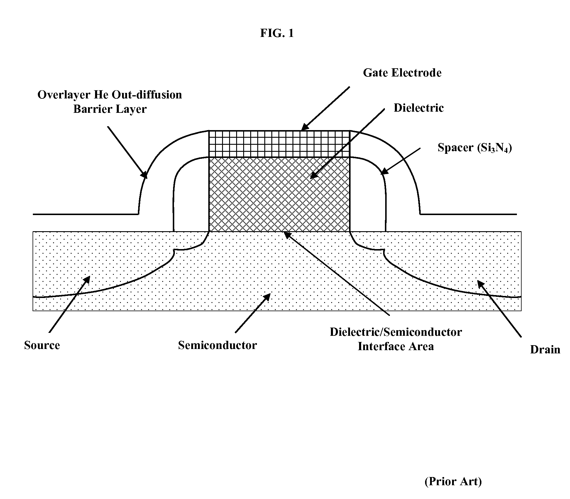
[0017]The mechanisms of aging of the dielectric / semiconductor interface involve de-passivation of the semiconductor-hydrogenous species bond followed by diffusion of the hydrogenous species away from the interface. In the case of irradiation, the fracture of Si—OH bonds and diffusion of H or H+ species through the dielectric network is of primary concern. In both processes involving release of the hydrogenous species it is clear that within some finite time the hydrogenous species must diffuse outside of a “capture radius.” Failing this the species could be re-trapped at the semiconductor ion / atom from which it has escaped. Clearly, if a physical mechanism can be found to reduce the probability that the hydrogenous species can escape the capture radius then the aging mechanism will be suppressed.

[0018]The present invention relies upon the observation that the structure of the dielectric contains substantial densities of interstitial voids and channels through which gases can diffuse...


PUM

PropertyMeasurementUnit
pressureaaaaaaaaaa
pressureaaaaaaaaaa
temperaturesaaaaaaaaaa

Abstract

In microelectronic circuits involving dielectric/semiconductor interfaces having interstitial sites in the dielectric, a method for hardening these interfaces by introducing a small atomic diameter inert gas into the interstitial sites.

Description

STATEMENT OF GOVERNMENT INTEREST[0001]The conditions under which this invention was made are such as to entitle the Government of the United States under paragraph I(a) of Executive Order 10096, as represented by the Secretary of the Air Force, to the entire right, title and interest therein, including foreign rights.BACKGROUND OF THE INVENTION[0002]The present invention is generally related to methods for enhancing the reliability of microelectronic circuits, and in particular, to minimizing induced aging from both electrical stress and radiation on devices and circuits due to the atomic mismatch at the interface of semiconductor / dielectric materials.[0003]A variety of physical phenomena contributes to the degradation of the fundamental electronic devices making up microelectronic circuits. One of the basic devices in any microelectronic circuit is a field effect transistor (FET). It will be used here to illustrate the degradation problem. The primary mechanism of degradation of FE...

Claims


Application Information

Patent Timeline
Patent Type & Authority Patents(United States)
IPC IPC(8): H01L21/469
CPCH01L21/26506H01L21/28176H01L21/3003H01L21/3115H01L21/31155H01L21/76825H01L21/76826H01L21/76829
Inventor DEVINE, RODERICK A. B.HUGHES, HAROLD L.REVESZ, AKOS G.
Owner THE GOVERNMENT OF THE UNITED STATES AS REPSESENTED BY THE SEC OF THE AIR FORCE
Why Eureka
Try Eureka