
Method to improve gate dielectric quality for FinFET

a gate dielectric quality and gate dielectric technology, applied in the field of semiconductor device structure, can solve the problems of time-dependent dielectric breakdown, negative bias temperature instability and positive bias temperature instability improve the reliability of the finfet device, time-dependent dielectric breakdown, and improve the integrity of the gate dielectric integrity

Active Publication Date: 2018-03-06
SEMICON MFG INT (SHANGHAI) CORP +1
View PDF12 Cites 0 Cited by
  • Summary
  • Abstract
  • Description
  • Claims
  • Application Information

AI Technical Summary

Benefits of technology

Enhances the reliability and performance of FinFET devices by improving gate dielectric integrity, reducing time-dependent and bias temperature instabilities, and maintaining high drive current and low power consumption, effectively addressing the challenges faced by FinFET devices.

Problems solved by technology

The novel method of introducing fluorine ions into the fin of a FinFET device results in an improvement in gate dielectric integrity, time-dependent dielectric breakdown, negative bias temperature instability and positive bias temperature instability of the FinFET device.

Method used


Image

  • Method to improve gate dielectric quality for FinFET
  • Method to improve gate dielectric quality for FinFET
  • Method to improve gate dielectric quality for FinFET

Examples


Embodiment Construction

[0037]In the following description, numerous specific details are provided for a thorough understanding of the present invention. However, it should be appreciated by those of skill in the art that the present invention may be realized without one or more of these details. In other examples, features and techniques known in the art will not be described for purposes of brevity.

[0038]It should be understood that the drawings are not drawn to scale, and similar reference numbers are used for representing similar elements. Embodiments of the invention are described herein with reference to cross-section illustrations that are schematic illustrations of idealized embodiments (and intermediate structures) of the invention. The thickness of layers and regions in the drawings may be exaggerated relative to each other for clarity. Additionally, variations from the shapes of the illustrations as a result, for example, of manufacturing techniques and / or tolerances, are to be expected. Thus, e...


PUM


Abstract

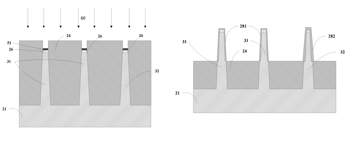
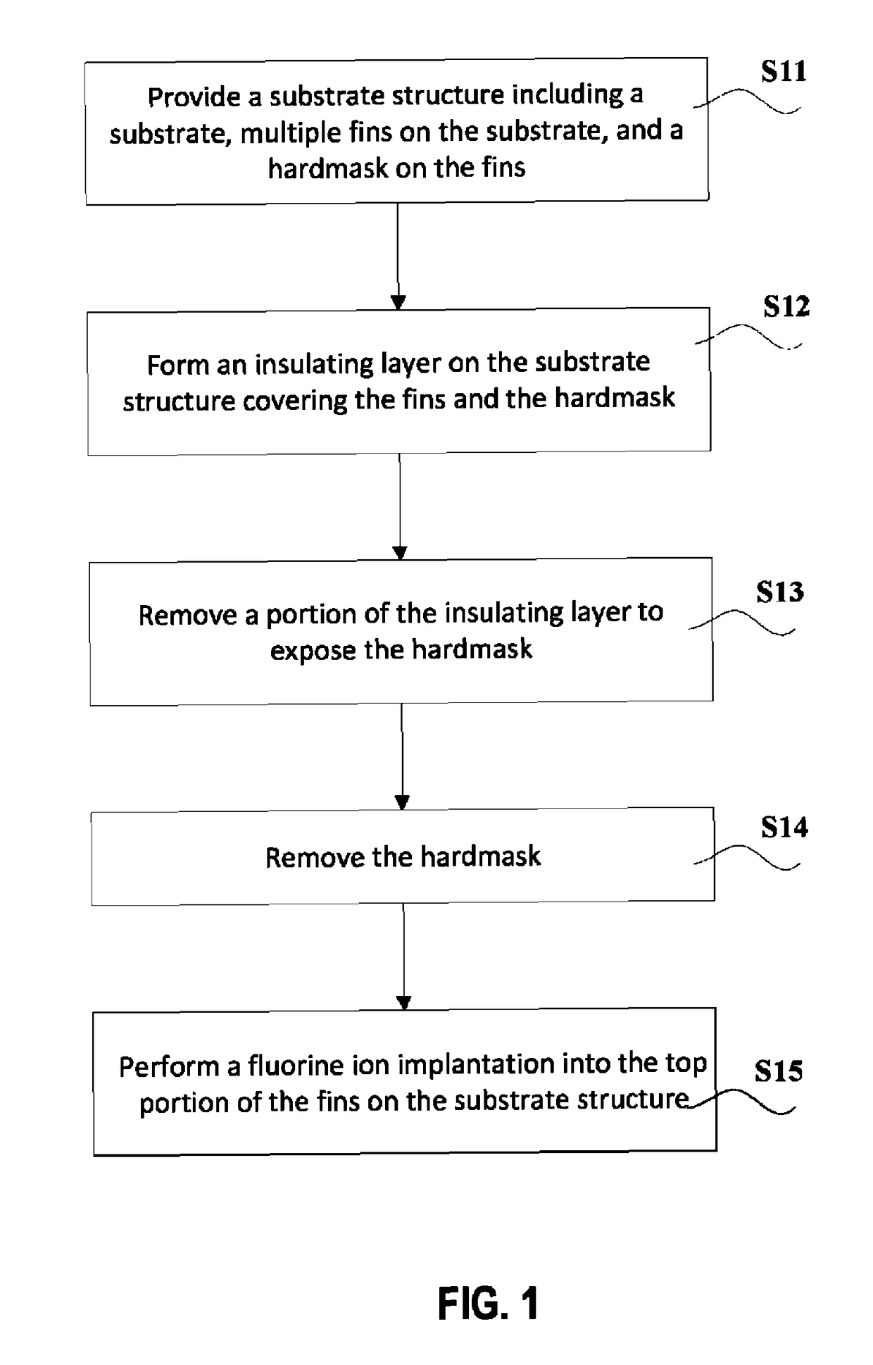
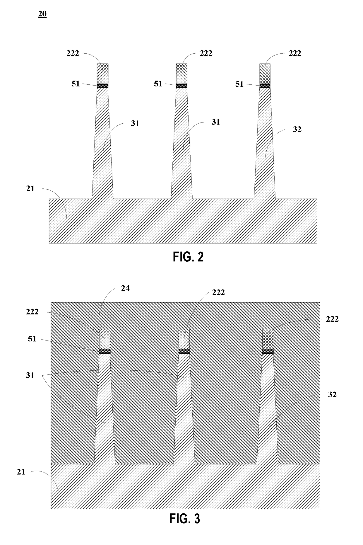
A method for manufacturing a semiconductor device includes providing a substrate structure comprising a substrate, a plurality of fins on the substrate and a hardmask on the fins, forming an insulating layer on the substrate structure covering the fins and the hardmask, removing a portion of the insulating layer by etching to expose the hardmask, removing the hardmask, and performing a fluorine ion implantation into a top portion of the fins. The implanted fluorine ions passivate dangling bonds in the top portion of the fins, thereby improving the reliability of the semiconductor device.

Description

CROSS-REFERENCES TO RELATED APPLICATIONS[0001]This application claims priority to Chinese patent application No. 201610018952.5, filed on Jan. 13, 2016, the content of which is incorporated herein by reference in its entirety.BACKGROUND OF THE INVENTION[0002]The present invention relates generally to semiconductor technology. Specifically, embodiments of the invention are directed to semiconductor device structures and a method of manufacturing the same.[0003]As the feature size of metal oxide semiconductor field-effect transistors (MOSFETs) continues to decrease, short channel effects have become a critical design issue due to the reduction in the size of the gate length. Fin Field-effect transistor (FinFET) devices exhibit excellent gate controllability on channel charge, superior electrostatic control capability, higher drive current and lower power consumption, so that the feature size of complementary metal oxide semiconductor (CMOS) devices can be further reduced to increase t...

Claims


Application Information

Patent Timeline
Patent Type & Authority Patents(United States)
IPC IPC(8): H01L21/8234H01L21/308H01L29/78H01L29/66H01L21/306H01L29/06H01L29/36H01L21/265
CPCH01L29/66795H01L21/265H01L21/3085H01L29/785H01L21/30625H01L29/0649H01L29/36H01L21/30604H01L21/26506H01L21/823431H01L27/0886H01L29/66803H01L29/7851
Inventor LI, YONG
Owner SEMICON MFG INT (SHANGHAI) CORP
Learn More