Semiconductor device

a technology of semiconductor devices and semiconductors, applied in semiconductor devices, semiconductor/solid-state device details, electrical apparatus, etc., can solve the problems affecting device performance, and achieve the effects of reducing current gain, avoiding negative bias temperature instability (nbti) degradation, and reducing current gain

Active Publication Date: 2007-11-01
MARLIN SEMICON LTD
View PDF3 Cites 0 Cited by
  • Summary
  • Abstract
  • Description
  • Claims
  • Application Information

AI Technical Summary

Benefits of technology

[0008] Therefore, it is an object of the present invention to provide a method for fabricating a semiconductor device. The fabricating method avoids the negative bias temperature instability (NBTI) degradation, which otherwise reduces the current gain and affects the device performance.
[0009] It is another object of the present invention to provide a semiconductor device that can avoid the negative bias temperature instability (NBTI) degradation, such that the device performance is improved.
[0022] According to the present invention, a tensile stress layer, a tensile stress layer and a compressive stress layer, or nothing, is formed on the I / O second-type MOS transistor. When the negative bias is applied on the substrate, H+ is not accumulated in the gate dielectric layer, thus the threshold voltage (Vt) shift effect does not occur. In other words, the negative bias temperature instability (NBTI) degradation in the conventional technique is effectively avoided. On the other hand, the method of the present invention does not increase the quantity of the photomasks used in the fabricating process, thus the present invention does not increase any additional fabricating cost.

Problems solved by technology

The fabricating method avoids the negative bias temperature instability (NBTI) degradation, which otherwise reduces the current gain and affects the device performance.

Method used


Image

  • Semiconductor device
  • Semiconductor device
  • Semiconductor device

Examples


Embodiment Construction

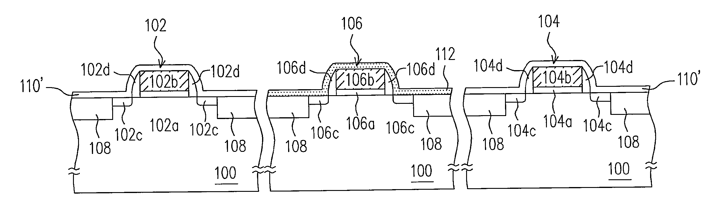
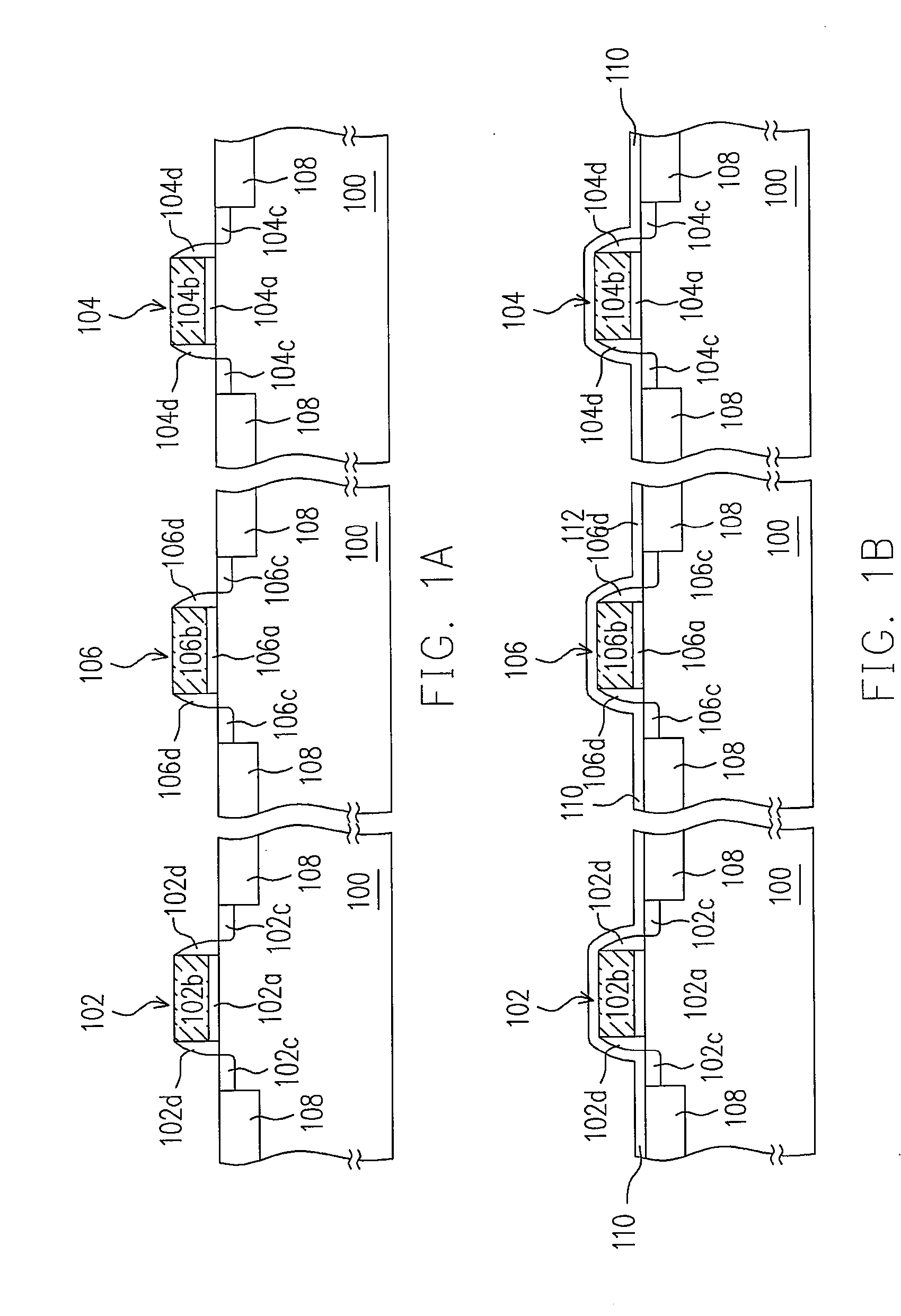
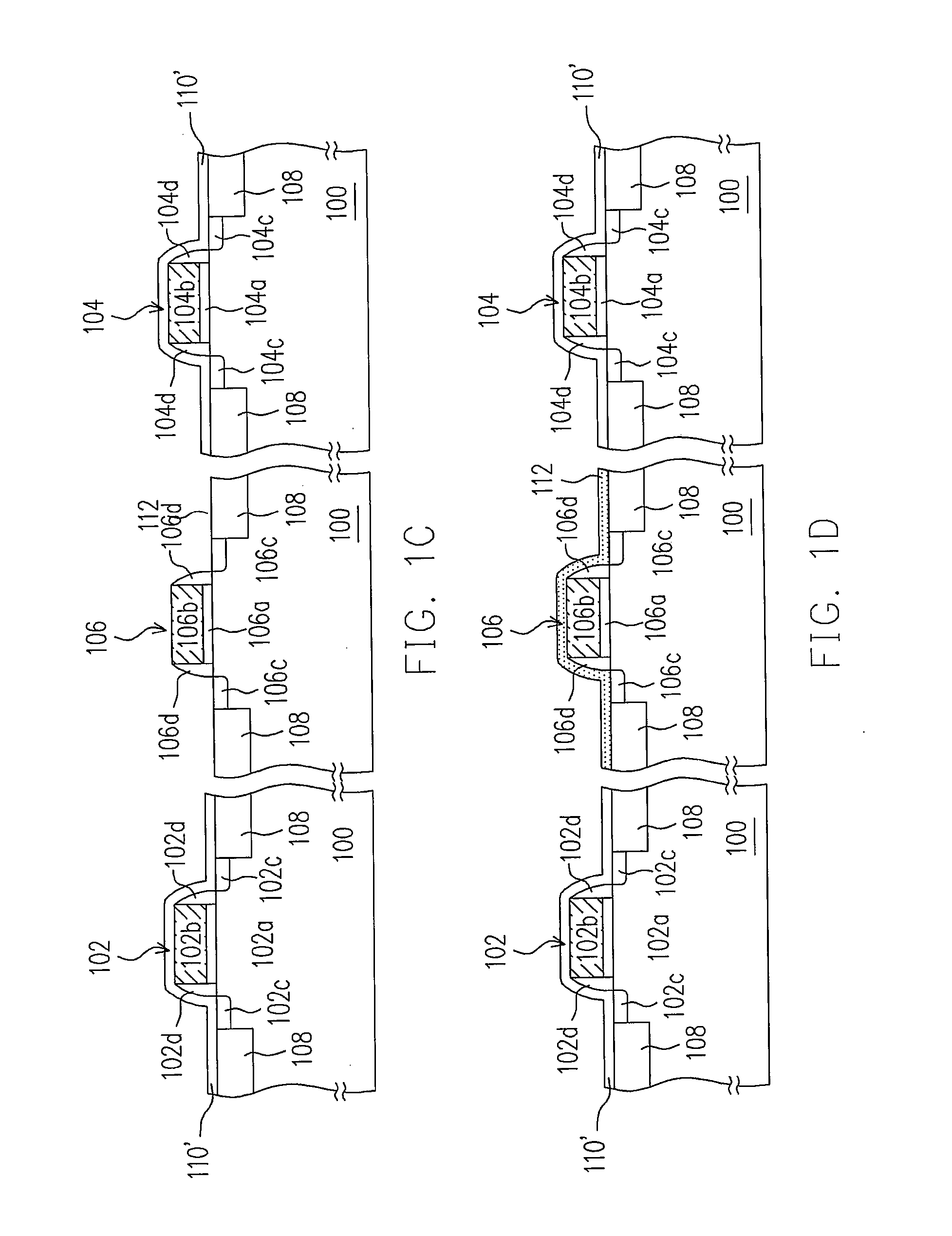
[0028]FIG. 1A-1D are cross-sectional views illustrating a method for fabricating a semiconductor device according to an embodiment of the present invention.

[0029] First, referring to FIG. 1A, a substrate 100 is provided. A first-type MOS transistor 102, an input / output (I / O) second-type MOS transistor 104, and a core second-type MOS transistor 106 are formed on the substrate 100. In addition, the first-type MOS transistor 102, the I / O second-type MOS transistor 104, and the core second-type MOS transistor 106 are separated from each other by an isolation structure 108. Here, the isolation structure 108 may be a shallow trench isolation (STI) structure.

[0030] The I / O second-type MOS transistor 104 is an input / output (I / O) MOS transistor, and the core second-type MOS transistor is a core MOS transistor. Wherein, the F first-type MOS transistor 102 may be an N-channel MOS (NMOS) transistor, and the I / O second-type MOS transistor 104 and the core second-type MOS transistor 106 may be ...


PUM


Abstract

A semiconductor device is provided herein, which includes a substrate having a first-type MOS transistor, an input / output (I / O) second-type MOS transistor, and a core second-type MOS transistor formed thereon. The semiconductor device further includes a first stress layer and a second stress layer. The first stress layer is disposed on the first-type MOS transistor, or on the first-type MOS transistor and the I / O second-type MOS transistor. The second stress layer is disposed on the core second-type MOS transistor.

Description

CROSS-REFERENCE TO RELATED APPLICATION [0001] This is a divisional application of an application Ser. No. 11 / 308,560, filed Apr. 7, 2006, now pending. The entirety of the above-mentioned patent application is hereby incorporated by reference herein and made a part of this specification.BACKGROUND OF THE INVENTION [0002] 1. Field of the Invention [0003] The present invention relates to an integrated circuit component and a method for fabricating the same, and more particularly, to a semiconductor device and a method for fabricating the same. [0004] 2. Description of the Related Art [0005] In the development of the integrated circuit components, high speed and low power electricity consumption are achieved by reducing the size of the component. However, the technique of reducing the component size is limited by the fabrication technique and high cost, thus a new technique of reducing the component size is desired to improve the device driving current. Accordingly, a method of using th...

Claims


Application Information

Patent Timeline
Patent Type & Authority Applications(United States)
IPC IPC(8): H01L27/092
CPCH01L21/823412H01L29/7842H01L21/823468
Inventor LEE, KUN-HSIENHUANG, CHENG-TUNGHUNG, WEN-HANTING, SHYH-FANNJENG, LI-SHIANCHENG, TZYY-MINGLANG, CHIA-WEN
Owner MARLIN SEMICON LTD
Why Eureka
Try Eureka