Fabrication method of semiconductor integrated circuit device

a technology of integrated circuit devices and fabrication methods, which is applied in the direction of semiconductor devices, electrical appliances, basic electric elements, etc., can solve the problems of cracking of semiconductor wafers, and achieve the effect of reducing the thickness of the wafer

Inactive Publication Date: 2008-11-18
RENESAS ELECTRONICS CORP
View PDF10 Cites 4 Cited by
  • Summary
  • Abstract
  • Description
  • Claims
  • Application Information

AI Technical Summary

Benefits of technology

[0016]Further, since a semiconductor wafer with a thickness of 100 μm or more, or 200 μm or more, causes less warping, it can be left for 4 hours or more, during which a spontaneous oxide layer is formed on the back surface of the semiconductor wafer, thereby avoiding the problem described above. However, it is necessary to leave the semiconductor wafer until the spontaneous oxide layer is formed, which inevitably lowers the TAT (turn around time).
[0017]It is an object of the present invention to provide a technique that is capable of stably releasing a chip from a dicing tape.
[0018]The invention has the further object of providing a technique that is capable of improving the yield of semiconductor products and shortening the TAT.
[0022]Further, according to another aspect of the invention, after reducing the thickness the back surface of a wafer, the wafer is forcibly oxidized or formed with an adhesion suppression layer, including formation of a silicon or acrylic base releasing agent layer on the back surface of the wafer. In this case, the strength upon separation can be optionally adjusted. On the other hand, compared with the use of an inorganic treating agent or treating solution, such as ozonized water, care should be taken for preventing contamination. However, a silicone type agent actually has been used generally so far in the field of semiconductors. Further, it can be used together with forcible oxidation. In this case, an advantage can be obtained in controlling the strength upon separation to an optimal value while keeping a state nearly equal with that of the existent spontaneous oxide layer.
[0026]That is, after reducing the thickness of the wafer, the back surface is forcibly oxidized or formed with an adhesion suppression layer thereby facilitating separation from the wafer retention member after dividing or substantially dividing the wafer into individual chips.

Problems solved by technology

However, when the thickness of a semiconductor wafer is reduced to less than 100 μm, a warping tends to be induced in the semiconductor wafer so as to cause a disadvantage in the handling or the transport of the semiconductor wafer in a subsequent step, to the extent that the semiconductor wafer sometimes cracks.

Method used


Image

  • Fabrication method of semiconductor integrated circuit device
  • Fabrication method of semiconductor integrated circuit device
  • Fabrication method of semiconductor integrated circuit device

Examples


embodiment 1

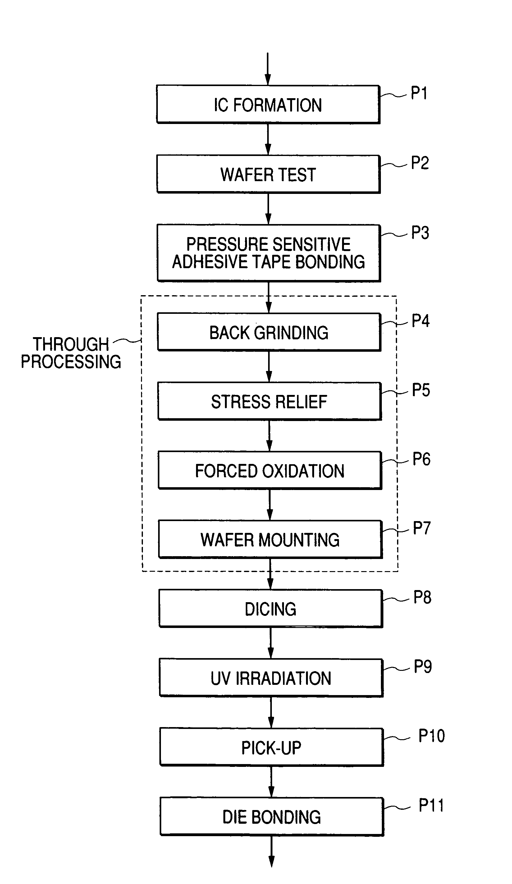
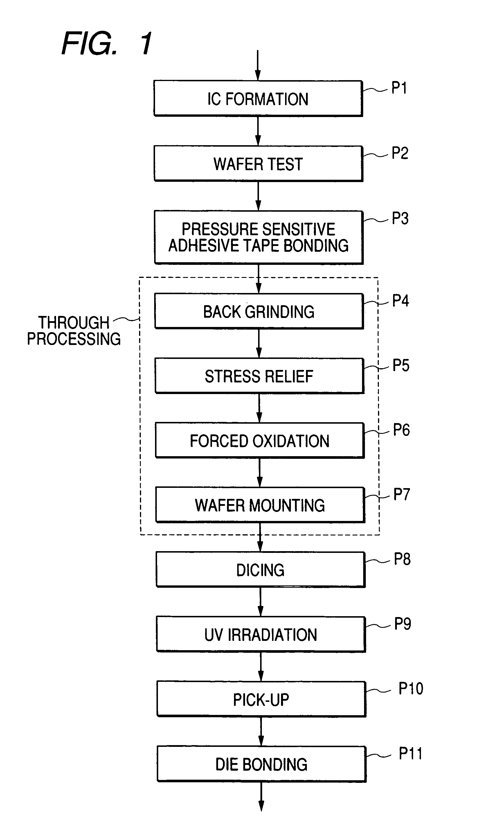
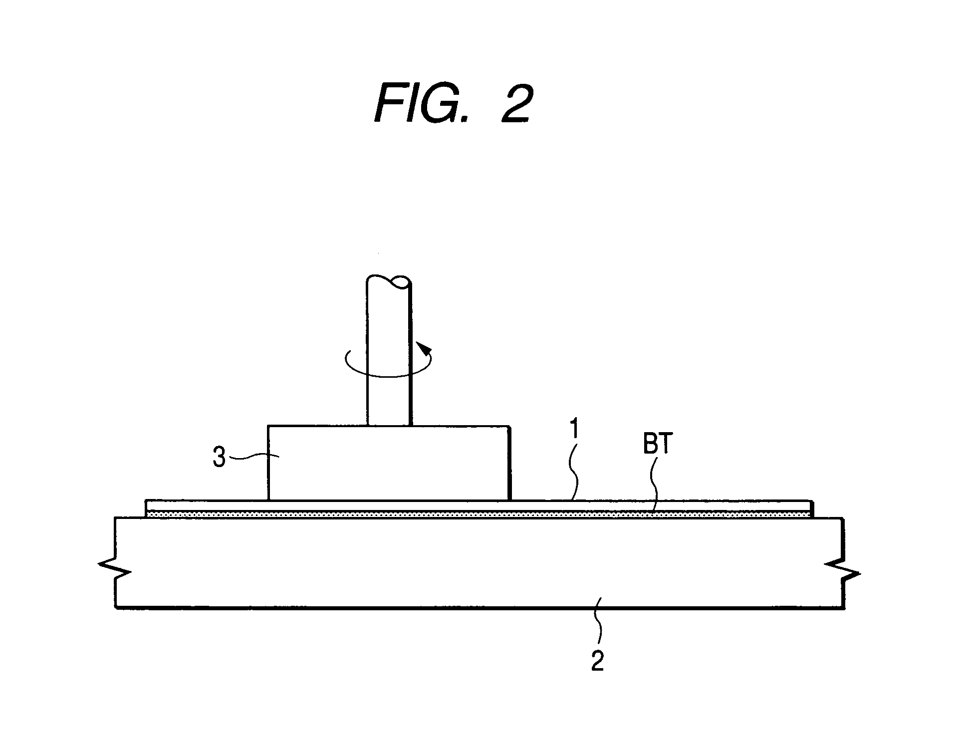
[0058]A method of fabrication of a semiconductor integrated circuit device according to Embodiment 1 will be described in the order of the steps thereof with reference to FIG. 1 to FIG. 13. FIG. 1 is a process flow chart showing a method of fabrication of the semiconductor integrated circuit device, FIG. 2 to FIG. 4 and FIG. 8(a), and FIG. 9 to FIG. 12 are side elevational views showing a main portion of the semiconductor integrated circuit device, FIG. 8(b) is an upper plan view showing a main portion of the semiconductor integrated circuit device, FIG. 5 is a diagram showing an ozonized water generation device, FIG. 6 is a diagram showing a cleaning portion of back grinding, FIG. 7 is a diagram showing the step of forming carbon dioxide-incorporated water, and FIG. 13 is a diagram showing a through processing apparatus from back grinding to wafer mounting. In the following description, only each of the steps, from back grinding after forming a circuit pattern on a semiconductor wa...

embodiment 2

[0091]In response to a demand for reducing the thickness of the chip, the semiconductor wafer is ground in back grinding to a thickness, for example, of less than 100 μm. The back surface of the ground semiconductor wafer comprises an amorphous layer / polycrystal layer / micro-crack layer / atom level strain layer (stress transfer layer) / complete crystal layer, in which the amorphous layer / polycrystal layer / micro-crack layer are crystal defective layers. The thickness of the crystal defective layer is, for example, about 1 to 2 μm.

[0092]In the case where a crystal defective layer is present on the back surface of the semiconductor wafer, this results in a problem in that there is a lowering of the flexion strength (stress value when the chip is destroyed upon application of a simple bending stress to the chip) of the chip divided from the semiconductor wafer into individual pieces. Lowering of the flexion strength appears remarkably in a chip with a thickness of less than 100 μm. Thus, s...


PUM


Abstract

A technique capable of stably releasing chips from a dicing tape, includes grinding a back surface of a semiconductor wafer, while adhering a pressure sensitive adhesive tape to a circuit forming surface of the semiconductor wafer formed with an integrated circuit, to achieve a predetermined thickness and forcibly oxidizing the back surface of the semiconductor wafer. Then, the pressure sensitive adhesive tape adhered to the circuit forming surface of the semiconductor wafer is released, and a dicing tape is adhered to the back surface of the semiconductor wafer. Further, the semiconductor wafer is divided by dicing it into individual chips, and then the back surface of the chip is pressed by way of the dicing tape, thereby releasing the chips from the dicing tape.

Description

CROSS-REFERENCE TO RELATED APPLICATION[0001]The present application claims priority from Japanese patent application No. 2004-036966, filed on Feb. 13, 2004, and Japanese patent application No. 2003-431866, filed on Dec. 26, 2003, the contents of both of which are hereby incorporated by reference into this application.BACKGROUND OF THE INVENTION[0002]The present invention concerns a method of fabrication of a semiconductor integrated circuit device; and, more particularly, it relates to a technique which is effective when applied to the fabrication of a semiconductor integrated circuit device including the processing, after substantial completion of the formation of a circuit pattern on a semiconductor wafer, from the back grinding step of grinding the back surface of a semiconductor wafer to the dicing step of cutting a semiconductor chip into individual chips, further including the die bonding step of picking-up and mounting the chip on a substrate.[0003]In the fabrication steps o...

Claims


Application Information

Patent Timeline
Patent Type & Authority Patents(United States)
IPC IPC(8): H01L21/00H01L21/301H01L21/304H01L21/306H01L21/314H01L21/316H01L21/46H01L21/52H01L21/60H01L21/68H01L21/78H01L21/82
CPCH01L21/02238H01L21/02255H01L21/314H01L21/6835H01L21/6836H01L21/78H01L21/31675H01L21/30625H01L21/31654H01L2221/6834H01L2221/68327H01L21/304H01L21/60
Inventor MIYAZAKI, CHUICHIABE, YOSHIYUKIUEMATSU, TOSHIHIDEKIMURA, MINORUSUZUKI, KAZUNARIODAGIRI, MASAOSUGA, HIDEYUKITAKATA, MANABU
Owner RENESAS ELECTRONICS CORP
Why Eureka
Try Eureka