
Method of supporting layout design of semiconductor integrated circuit

a technology of integrated circuits and layouts, applied in the direction of cad circuit design, program control, instruments, etc., can solve the problems of local arrangement and wiring congestion, affecting the timing convergence of layout design, so as to achieve the effect of reducing the timing convergence after layout design

Inactive Publication Date: 2013-07-30
RENESAS ELECTRONICS CORP
View PDF7 Cites 0 Cited by
  • Summary
  • Abstract
  • Description
  • Claims
  • Application Information

AI Technical Summary

Benefits of technology

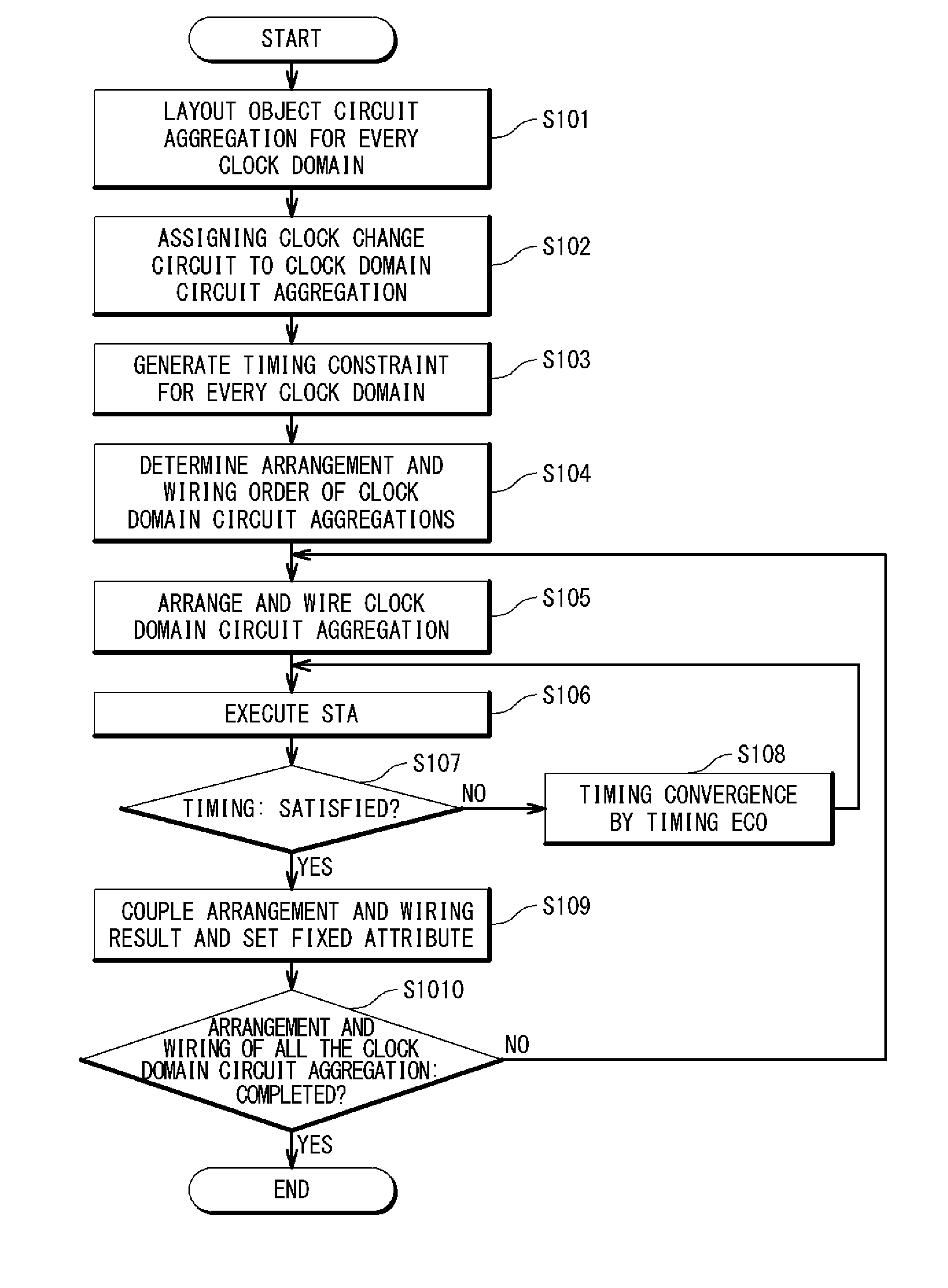
[0012]According to the present invention, a layout object circuit is divided every clock domains. By arranging and wiring the clock domain circuit aggregations from aggregation having severer timing, timing convergence of the path having the severer timing can be carried out primarily in a state of free area. As a result, TAT of the timing convergence after layout design can be shortened.

Problems solved by technology

As a result, a possibility increases that a local arrangement congestion and a wiring congestion which accompanies it and moreover the wiring detour occur.
Specifically, in a LSI circuit with five clock systems and 20,000,000 logic gates, the local arrangement and wiring congestion occur in about 10% of the chip and the wiring detour occurs with this.
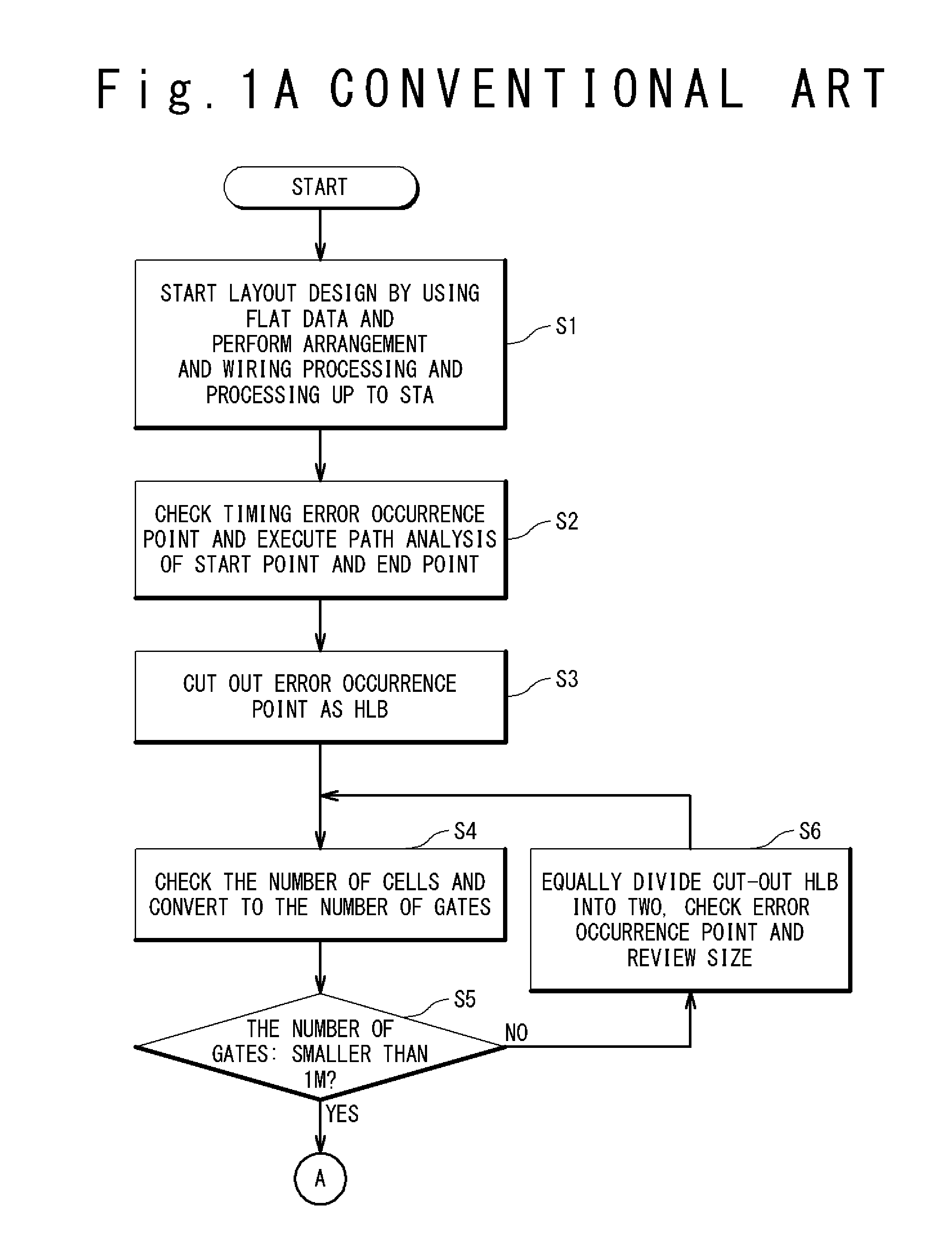
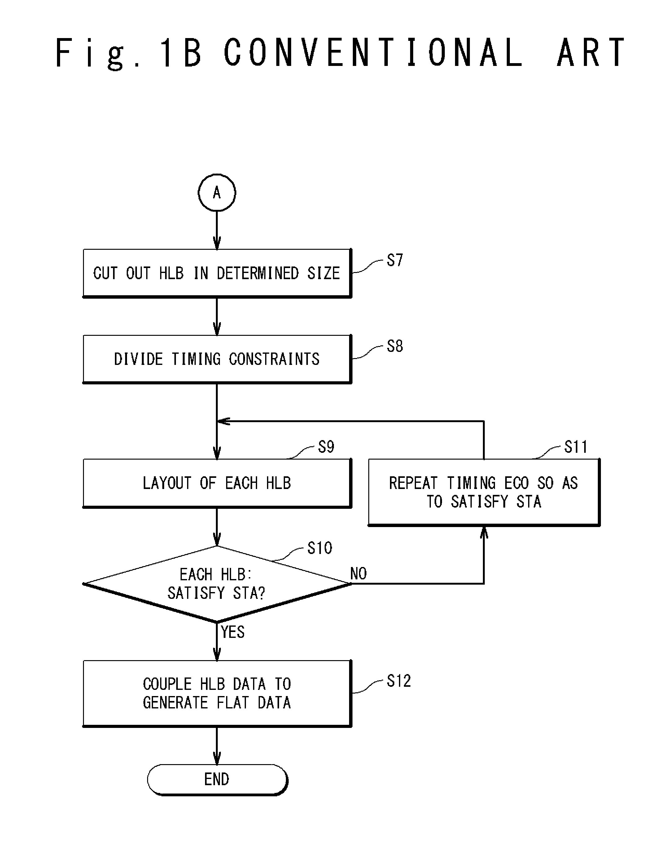
Therefore, when many timing errors occur as well as the wiring congestion in an initial stage of flat arrangement and wiring (the preprocessing for the hierarchy layout in the conventional technique), an area for size-up of a cell and an area for inserting a repeater for the purpose of the timing convergence are lacking in the HLB in case of the layout of HLB (in other words, a hierarchy layout) after the division into HLBs.
As a result, the timing convergence cannot be attained in the HLB, and the control flow returns to the start and needs the review of a floor plan.

Method used


Image

  • Method of supporting layout design of semiconductor integrated circuit
  • Method of supporting layout design of semiconductor integrated circuit
  • Method of supporting layout design of semiconductor integrated circuit

Examples


first embodiment

[0027]FIG. 2 is a block diagram showing a system configuration of the layout design supporting system according to a first embodiment. This system is provided with a computer terminal 10, a server 14, a storage unit 15 and a network 16. The storage unit 15 is contained in the server 14 to store an execution program. The server 14 is connected with the computer terminal 10 such as an engineering workstation through the network 16 such as the Internet. The execution program is stored in the storage unit 15 and is downloaded into the computer terminal 10 through the network 16. The execution program may be installed from a storage medium into the computer terminal 10. The downloaded program is stored in a local hard disk or a memory and so on in the computer terminal 10.

[0028]FIG. 3 is a flow chart showing an operation procedure of the present invention. The computer terminal 10 extracts circuits connected with each clock through a forward search of a net list of an LSI circuit from a ...

second embodiment

[0055]The system configuration of a second embodiment is the same as that of the first embodiment and the description thereof is omitted. In the first embodiment, the arrangement and wiring order of the clock domain circuit aggregations is determined in order from the clock with the higher frequency based on the timing constraint of the LSI circuit (Step S104). In the second embodiment, the same arrangement and wiring order is assigned to a plurality of clock domain circuit aggregations such that the clock domain circuit aggregations are arranged and wired at a same time. The clock domain circuit aggregations of the same order can be specified by an external input.

[0056]By collectively carrying out the arrangement and wiring to the plurality of clock domain circuit aggregations which are related to each other, the arrangement and wiring are carried out in consideration of the connection relation of the clock domain circuit aggregations to facilitate the timing convergence of the clo...


PUM


Abstract

In a method of supporting a layout design, a net list of an integrated circuit is divided into net lists of clock domain circuit aggregations. A timing constraint is generated to each of the clock domain circuit aggregations. An arrangement order of the clock domain circuit aggregations is determined to satisfy the timing constraint. A layout of the integrated circuit is generated by carrying out arrangement and wiring of the clock domain circuit aggregations based on the arrangement order.

Description

CROSS REFERENCE[0001]This patent application claims a priority on convention based on Japanese Patent Application No. JP 2011-38869. The disclosure thereof is incorporated herein by reference.TECHNICAL FIELD[0002]The present invention is related to a technique of a layout design of a semiconductor integrated circuit (especially, LSI circuit), and for example, related to a layout design technique for timing convergence.BACKGROUND ART[0003]In a technique of a layout design of an LSI circuit, the need of a method of supporting a layout design increases in which the timing convergence can be attained without increasing TAT (Turn Around Time) with increase of a circuit scale and operation speed in the LSI circuit.[0004]Patent Literature 1 (especially, reference to FIG. 3 and page 2) describes a technique for sufficiently shortening TAT by a hierarchy layout design method in case of development of an LSI circuit. In this technique, preprocessing is carried out to extract a timing error pa...

Claims


Application Information

Patent Timeline
Patent Type & Authority Patents(United States)
IPC IPC(8): G06F17/50
CPCG06F17/5068G06F30/39
Inventor OKABE, HIDEYUKI
Owner RENESAS ELECTRONICS CORP
Learn More