Aluminum nitride passivated phosphors for electroluminescent displays
a technology of passivating phosphors and electroluminescent displays, which is applied in the direction of discharge tubes luminescnet screens, instruments, natural mineral layered products, etc., can solve the problems of reducing reducing the efficiency with which electrons interact with the activator species in the phosphor to emit light, etc., to reduce the realizable luminance of the phosphor, the effect of preventing or minimizing the effect of any
- Summary
- Abstract
- Description
- Claims
- Application Information
AI Technical Summary
Benefits of technology
Problems solved by technology
Method used
Image
Examples
example 1
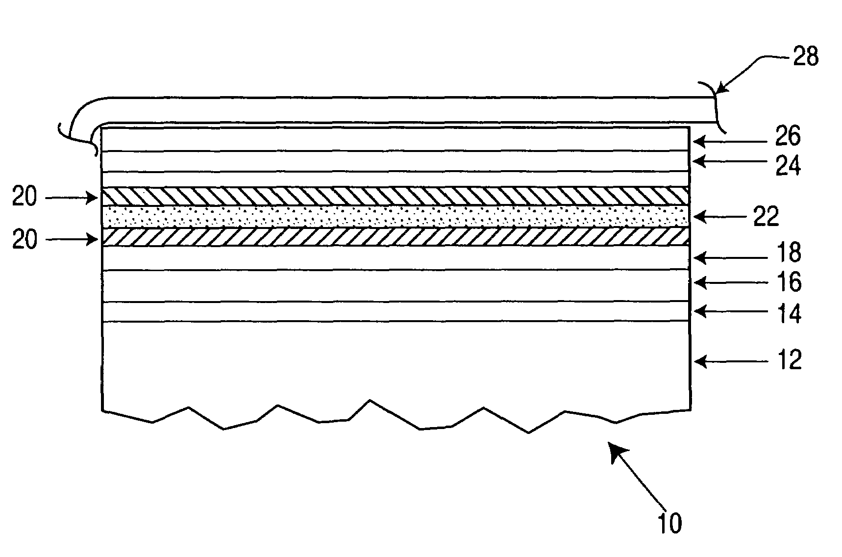
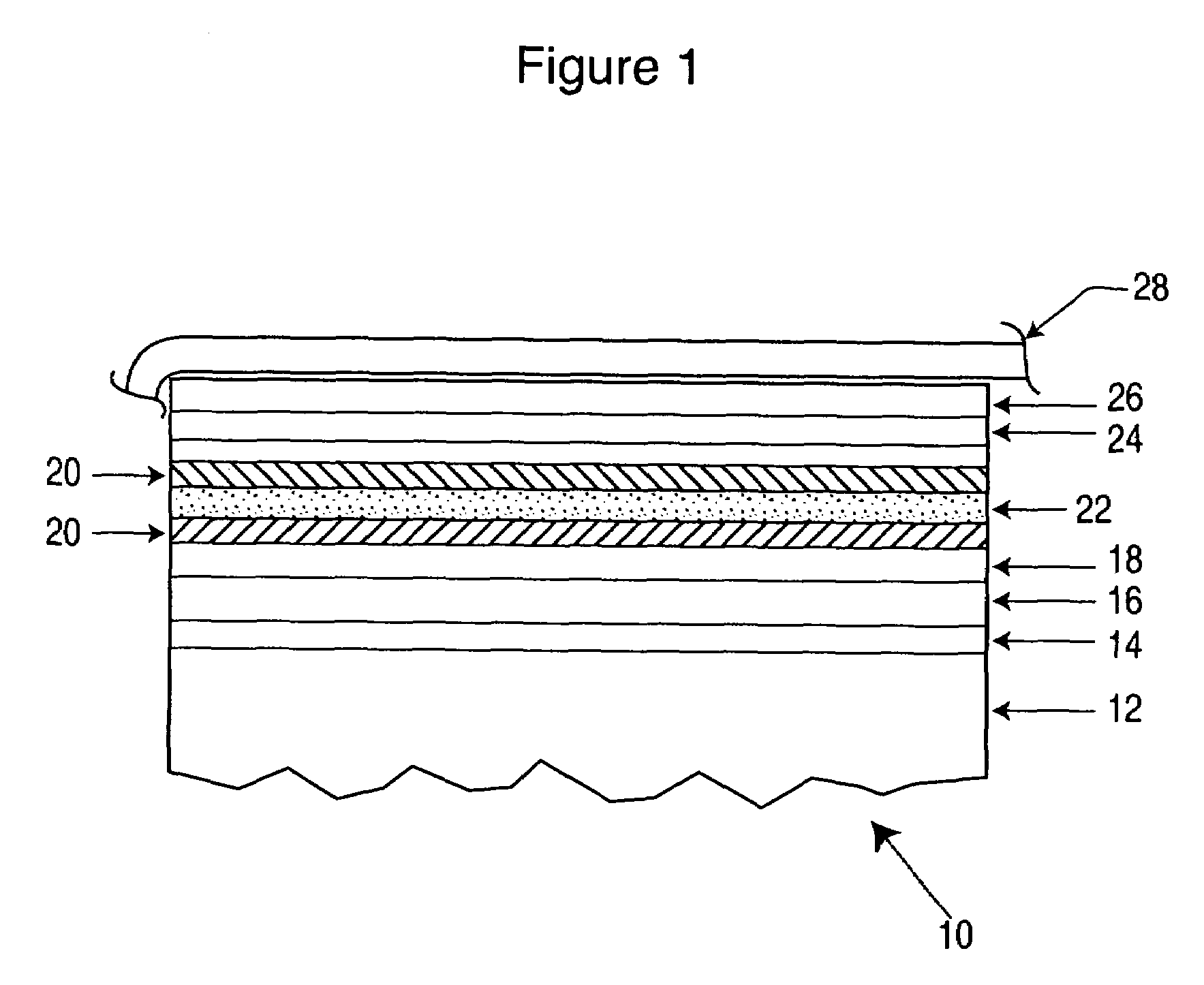
[0080]A thick film dielectric electroluminescent device incorporating thin film phosphor layers comprising barium thioaluminate activated with europium was constructed. The thick film substrate comprised a 5 cm by 5 cm alumina substrate having a thickness of about 0.1 cm. A gold electrode was deposited on the substrate, followed with a thick film high dielectric constant dielectric layer in accordance with the methods exemplified in Applicant's co-pending international application PCT CA00 / 00561 filed May 12, 2000 (the entirety of which is incorporated herein by reference). A thin film dielectric layer consisting of barium titanate, with a thickness of about 100-200 nanometers, was deposited on top of the thick film dielectric layer using the sol gel technique described in Applicant's co-pending U.S. patent application Ser. No. 09 / 761,971 filed Jan. 17, 2001 (the entirety of which is incorporated herein by reference). A 400 nm thick barium magnesium thioaluminate phosphor film activ...
example 2
[0084]A device was constructed similar to that of example 1, except that the aluminum nitride dielectric layer was replaced by an alumina layer of similar thickness. The luminance data for this device is also shown in FIG. 3 and shows a luminance of about 120 candelas per square meter at 60 volts above its threshold voltage of 160 volts. The lower threshold voltage of the device with the aluminum nitride layer is attributed to the higher dielectric constant for aluminum nitride as compared to alumina. The luminance at 60 volts above the threshold voltage for the device with the aluminum nitride layer is about 40% higher than that for the device with the aluminum oxide layer.
example 3
[0085]A device was constructed similar to that of example 1, except that the phosphor layer was sputtered terbium activated zinc sulfide rather than europium activated barium thioaluminate, with a thickness of about 700 nanometers. The luminance as a function of voltage for this device under the same test conditions is shown in FIG. 4. As can be seen from the data the luminance at 60 volts above the threshold voltage of 170 volts was about 3000 candelas per square meter.
PUM
| Property | Measurement | Unit |
|---|---|---|
| thickness | aaaaa | aaaaa |
| thick | aaaaa | aaaaa |
| pressure | aaaaa | aaaaa |
Abstract
Description
Claims
Application Information
 - R&D
- Intellectual Property
- Life Sciences
- Materials
- Tech Scout
- Unparalleled Data Quality
- Higher Quality Content
- 60% Fewer Hallucinations
Browse by: Latest US Patents, China's latest patents, Technical Efficacy Thesaurus, Application Domain, Technology Topic, Popular Technical Reports.
© 2025 PatSnap. All rights reserved.Legal|Privacy policy|Modern Slavery Act Transparency Statement|Sitemap|About US| Contact US: help@patsnap.com


