Direct write nanolithography using heated tip

a nanolithography and tip technology, applied in the field of nanolithography, can solve the problems of prohibitively expensive photomasks, difficult optical lithography, and inability to manufacture photomasks,

Inactive Publication Date: 2008-10-21
GEORGIA TECH RES CORP
View PDF8 Cites 7 Cited by
  • Summary
  • Abstract
  • Description
  • Claims
  • Application Information

AI Technical Summary

Problems solved by technology

However, as device dimensions shrink below 100 nm in size, optical lithography becomes increasingly difficult.
A major problem with optical lithography is in the fabrication of the photomasks that generate the optical patterns used in forming desired physical patterns.
As device dimensions shrink, photomasks become prohibitively expensive due to the low yields associated with producing such technically demanding photomasks.
Direct-write electron beam lithography is limited because it uses a serial writing style that limits throughput and also because increasing exposure times are required as feature sizes are reduced and accelerating potentials are increased.
Also, due to their highly complex nature, the development and final costs of advanced electron beam patterning systems are extremely high.
Once fabricated, integrated circuit chips are not easily post-processed, especially given the high temperatures and harsh chemical conditions that conventional patterning systems expose the chip to.
One strategy to post-processing has been complete encapsulation of the circuit elements, but this does not allow the circuit itself to be modified.
While there are a number of nanometer-scale manufacturing techniques that exploit the AFM, there remain several unmet needs.
While sub-100 nm resolution is possible with a number of techniques, the writing speed is a significant challenge, with typical tip speeds in the range 0.1-1 nm / sec.
Furthermore, AFM writing techniques offer little three-dimensionality, with most writing resulting in very thin marks or, at best, digging or building that offers little control in the z-direction.

Method used


Image

  • Direct write nanolithography using heated tip
  • Direct write nanolithography using heated tip
  • Direct write nanolithography using heated tip

Examples


Embodiment Construction

[0030]A preferred embodiment of the invention is now described in detail. Referring to the drawings, like numbers indicate like parts throughout the views. As used in the description herein and throughout the claims, the following terms take the meanings explicitly associated herein, unless the context clearly dictates otherwise: the meaning of “a,”“an,” and “the” includes plural reference, the meaning of “in” includes “in” and “on.”

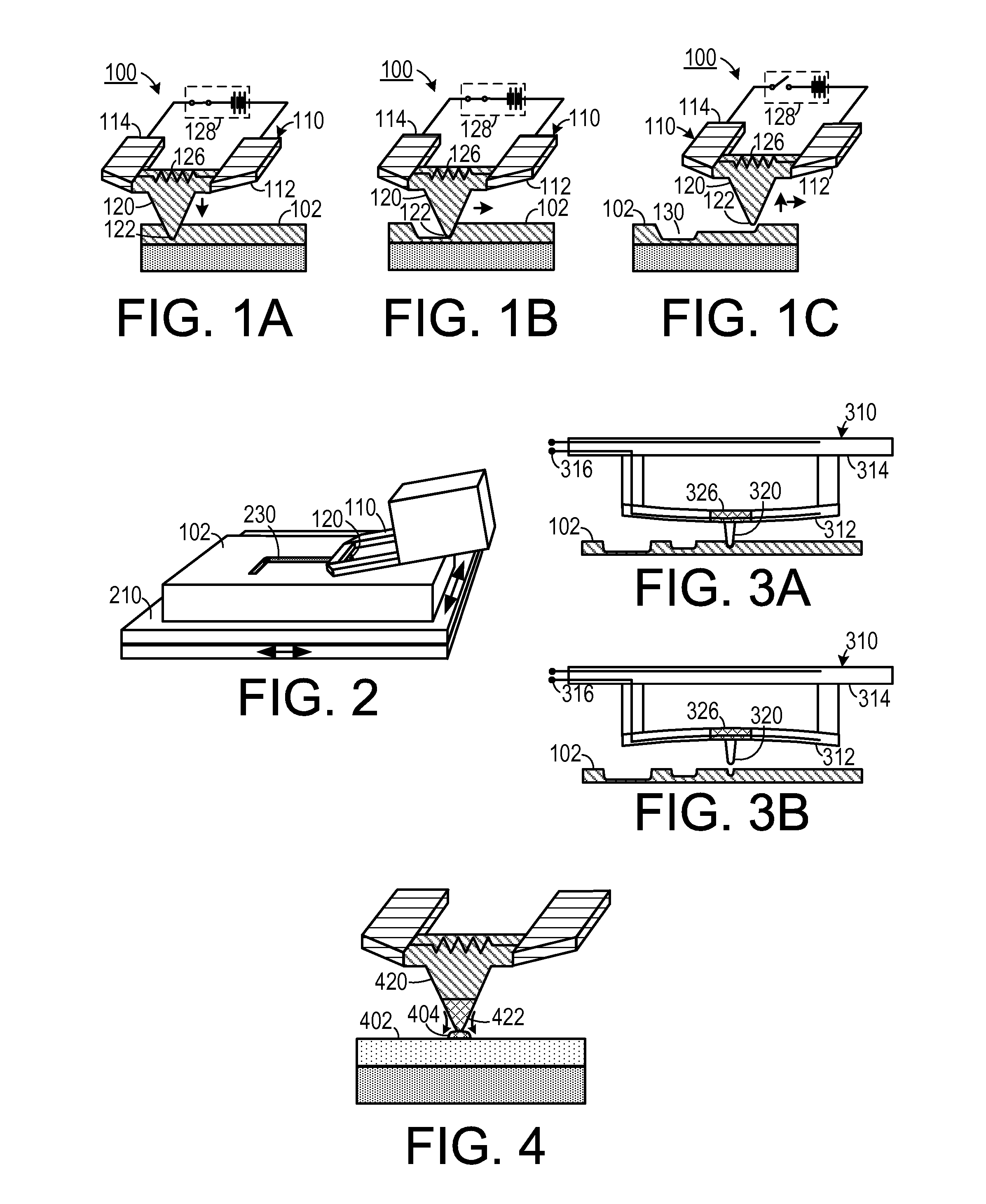
[0031]One embodiment includes a system and a method for sculpting a surface at the nano-scale. The embodiment includes a probe that can be heated to a temperature that causes material near the surface to decompose. The tip of the probe is brought close to, or in contact with, the surface so as to cause material adjacent the tip of the probe to decompose. As shown in FIGS. 1A-1C, one embodiment includes a nano-sculpting device 100 that employs a probe 120 having a probe tip 122 and a heating element 126 associated therewith. The heating element 126 may be...


PUM

PropertyMeasurementUnit
wavelengthsaaaaaaaaaa
sizeaaaaaaaaaa
roughnessaaaaaaaaaa

Abstract

A device for sculpting a substrate includes a vertically displaceable probe having a nano-scale dimensioned probe tip. A displacement mechanism is configured to adjust a vertical displacement between the probe tip and the substrate. A heating mechanism selectively heats the probe tip to a preselected temperature that is sufficient to cause a portion of the substrate in contact with the probe tip to decompose.

Description

CROSS-REFERENCE TO RELATED APPLICATION[0001]This application claims the benefit of U.S. Provisional Patent Application Ser. No. 60 / 712,622, filed Aug. 30, 2006, the entirety of which is hereby incorporated herein by reference.BACKGROUND OF THE INVENTION[0002]1. Field of the Invention[0003]The present invention relates to nanolithography and, more specifically, to a method for sculpting two-dimensional and three-dimensional nano-scale patterns using a heatable probe.[0004]2. Description of the Prior Art[0005]Small scale patterning and sculpting of surfaces to produce devices as diverse as semiconductors or biological systems is typically accomplished using one of three methods: (1) optical lithography using projection exposure tools at wavelengths ranging from 365 nm to 13 nm, (2) direct write electron beam lithography, and (3) imprint or embossing lithography.[0006]Optical lithography produces a large volume of micro-scale and nano-scale devices. However, as device dimensions shrink...

Claims


Application Information

Patent Timeline
Patent Type & Authority Patents(United States)
IPC IPC(8): G01N13/16G01B5/28G01B7/34G12B21/02G01Q80/00
CPCB82Y10/00G03F7/0002B82Y40/00G01Q80/00
Inventor KING, WILLIAM P.HENDERSON, CLIFFORD L.
Owner GEORGIA TECH RES CORP
Why Eureka
Try Eureka