Stacked chip semiconductor device
a semiconductor device and stacked chip technology, applied in semiconductor devices, semiconductor/solid-state device details, electrical equipment, etc., can solve the problems of low area efficiency of chip layout, difficult to miniaturize device may not be cost-effective, so as to reduce power consumption of stacked chip semiconductor devices, the effect of miniaturization of electronic systems and reducing power consumption
- Summary
- Abstract
- Description
- Claims
- Application Information
AI Technical Summary
Benefits of technology
Problems solved by technology
Method used
Image
Examples
first embodiment
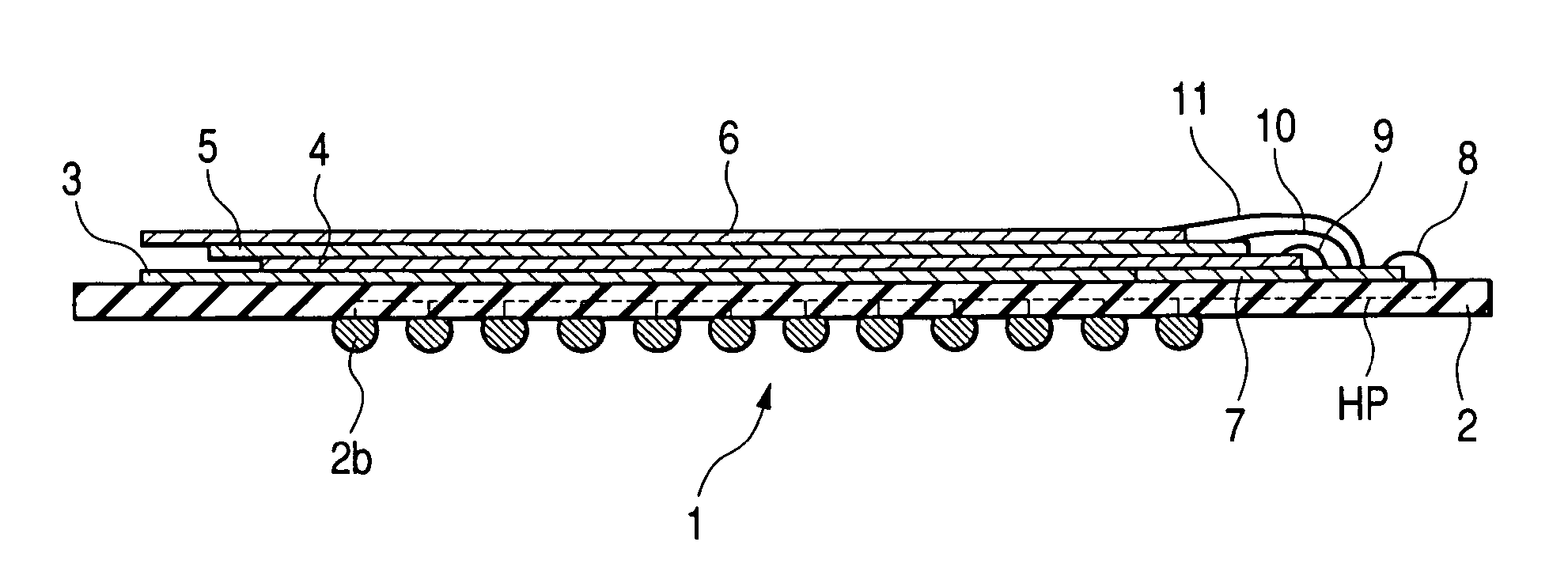
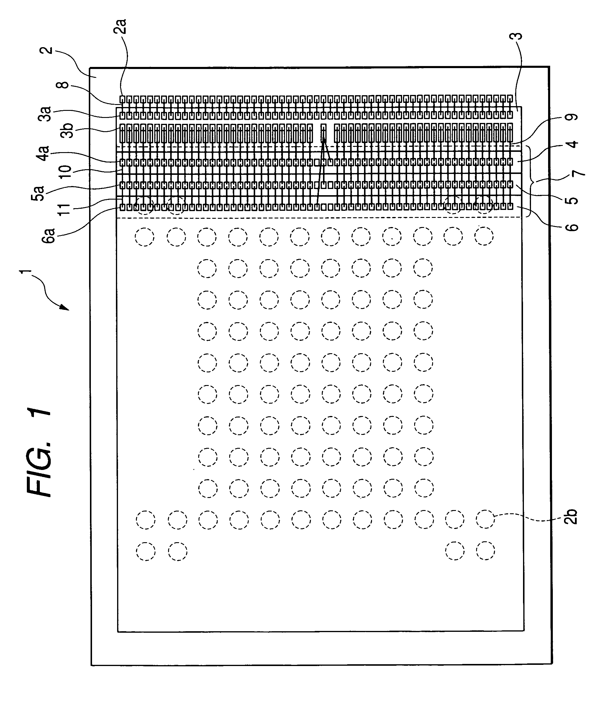
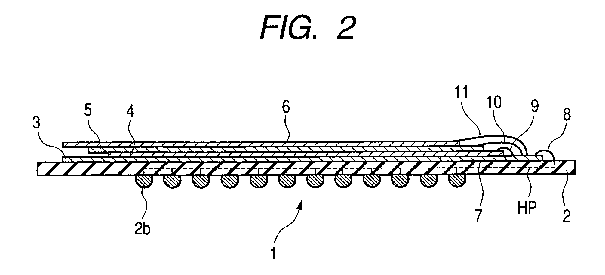
[0035]FIG. 1 is a top view of a stacked chip semiconductor device according to a first embodiment of the present invention, FIG. 2 is a sectional view of the stacked chip semiconductor device of FIG. 1, FIG. 3 illustrates an interface circuit in the stacked chip semiconductor device of FIG. 1, FIG. 4 is a circuit diagram of an ESD protection circuit and an input buffer which are incorporated in the interface circuit of FIG. 3, and FIG. 5 is a circuit diagram of an output buffer incorporated in the interface circuit of FIG. 3.
[0036]In the first embodiment, a stacked chip semiconductor device 1 consists of a BGA (Ball Grid Array) as a kind of surface mount CSP. As shown in FIGS. 1 and 2, the semiconductor device 1 has a printed wiring board 2, for example, made of BT (Bismaleimide Triazine). On the back of the printed wiring board 2 is an array of electrodes for connection.
[0037]The printed wiring board 2 has a stacked structure in which semiconductor chips 3 to 6 are stacked in the c...
second embodiment
[0080]FIG. 7 is a top view of a stacked chip semiconductor device according to the second embodiment of the present invention; and FIG. 8 is a sectional view of the stacked chip semiconductor device of FIG. 7.
[0081]As shown in FIGS. 7 and 8, in the second embodiment, the stacked chip semiconductor device 1b consists of a BGA with a stacked structure. Like the first embodiment (see FIGS. 1 and 2), the stacked chip semiconductor device 1b includes a printed wiring board 2, solder bumps 2b, semiconductor chips 3 to 6, bonding wires 8a and bonding wires 9 to 11. The difference from the first embodiment is the layout of the interface circuit of the semiconductor chip 3.
[0082]The interface circuit 7 is located not on the periphery of the external connection electrodes 3a and internal connection electrodes 3b on the semiconductor chip 3, but on the side facing the side where the external connection electrodes 3a are located.
[0083]The connection electrodes are located on the back surface of...
third embodiment
[0090]FIG. 9 is a sectional view of a stacked chip semiconductor device according to the third embodiment of the present invention.
[0091]In the third embodiment, a stacked chip semiconductor device 1c is the same as in the first embodiment except that a semiconductor chip (semiconductor chip with ESD protection) 27 is newly added and semiconductor chips 31, and 4 to 6 only have memory sections.
[0092]As shown in FIG. 9, in the stacked chip semiconductor device 1c, the connection electrodes are located on the back surface of the printed wiring board 2 as an array. The semiconductor chips 31, and 4 to 6 are stacked in the center of the main surface of the printed wiring board 2 and the additional semiconductor chip 27, on which an interface circuit 7 (FIG. 3) is structured, lies over the semiconductor chip 6.
[0093]The bonding electrodes 2a are located on the right side of the periphery of the main surface of the printed wiring board 2. The bonding electrodes 2a are electrically connect...
PUM
 Abstract
Description
Claims
Application Information
 - R&D
- Intellectual Property
- Life Sciences
- Materials
- Tech Scout
- Unparalleled Data Quality
- Higher Quality Content
- 60% Fewer Hallucinations
Browse by: Latest US Patents, China's latest patents, Technical Efficacy Thesaurus, Application Domain, Technology Topic, Popular Technical Reports.
© 2025 PatSnap. All rights reserved.Legal|Privacy policy|Modern Slavery Act Transparency Statement|Sitemap|About US| Contact US: help@patsnap.com


