Solid-state image-sensing device

a solid-state image and image sensing technology, applied in the field of solid-state image sensing devices, can solve the problems of calibration noise data not being acquired by ordinary image sensing, and the production of fixed-pattern noise components among pixels, and achieve the effect of variable sensitivity among individual pixels

Inactive Publication Date: 2008-08-26
KONICA MINOLTA INC +1
View PDF14 Cites 1 Cited by
  • Summary
  • Abstract
  • Description
  • Claims
  • Application Information

AI Technical Summary

Benefits of technology

[0008]object of the present invention is to provide a solid-state image-sensing device in which variations in sensitivity among individual pixels can be corrected for without irradiation with uniform light.
[0010]With the solid-state image-sensing device configured as described above, when sensed-image data is acquired, an output commensurate with the amount of light incident on the photoelectric converter is obtained and, when noise data is acquired, an output unrelated to the amount of light incident on the photoelectric converter is obtained. Thus, by performing correction by using those data, it is possible to correct for variations in sensitivity among individual pixels without irradiation with uniform light. This eliminates the need to previously acquire calibration noise data. Moreover, even in the presence of variations in temperature and other conditions, calibration noise data can be acquired on a real-time basis. Thus, it is no longer necessary to give a frame memory a large capacity to store therein sensed-image data acquired under a plurality of sets of conditions.
[0013]The solid-state image-sensing device configured as described above may be provided with, as the pixel circuit, a plurality of such pixel circuits arrayed in a matrix. In that case, the operation for acquiring one frame worth of sensed-image data and the operation for acquiring one line worth of noise data are performed alternately while the line on which the one line worth of noise data is acquired is varied sequentially and, after noise data on all lines of one frame are acquired, based on the noise data on all the lines, one frame worth of noise data are generated. This permits image sensing at a higher frame rate than when the operation for acquiring one frame worth of sensed-image data and the operation for acquiring one frame worth of noise data are performed alternately, and permits acquisition of noise data without loss of frames as occurs when the operation for acquiring a plurality of frames worth of sensed-image data and the operation for acquiring one frame worth or a plurality of frames worth of noise data are performed alternately.
[0014]Alternatively, the solid-state image-sensing device configured as described above may be provided with, as the pixel circuit, a plurality of such pixel circuits arrayed in an n-row, m-column matrix (where n and m are natural numbers). In this case, after one frame worth of sensed-image data are acquired, first, sensed-image data on line k (where k is a natural number fulfilling 1≦k≦n) are read out, then noise data on line k only is acquired, then the operation for reading one frame worth of data sequentially from line 1 is repeated while the value of k is varied sequentially, and, after noise data on all lines of one frame are acquired, based on the noise data on all the lines, one frame worth of noise data are generated. Thus, as compared with when no noise data is acquired, the only increase in the length of time for which exposure cannot be performed is the period for reading out the one line worth of sensed-image data on line k plus the period for acquiring the one line worth of noise data on line k. This helps minimize dead time.

Problems solved by technology

In such logarithmic-conversion solid-state image-sensing devices, variations in threshold voltage among individual MOS transistors for logarithmic conversion produce variations in sensitivity among individual pixels, and eventually produce fixed-pattern noise components among pixels.
With these logarithmic-conversion solid-state image-sensing devices that use, as calibration noise data for correcting actually sensed images, sensed-image data obtained under irradiation with uniform light, however, the calibration noise data cannot be acquired by ordinary image sensing.

Method used


Image

  • Solid-state image-sensing device
  • Solid-state image-sensing device
  • Solid-state image-sensing device

Examples


first embodiment

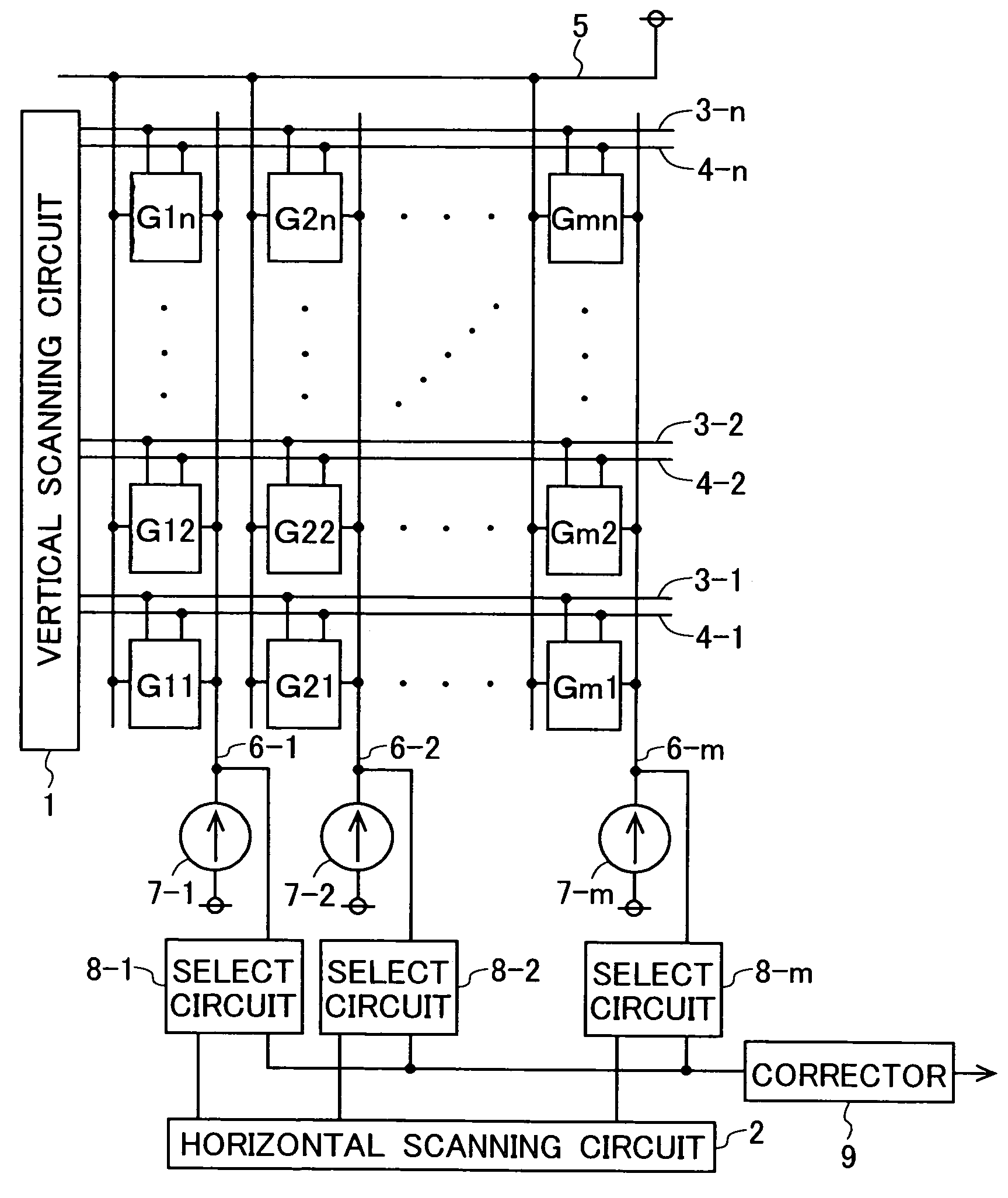
[0041]In the present invention, under the control of the timing generator and the signal controller mentioned above, an operation for acquiring one frame worth of sensed-image data and an operation for acquiring one frame worth of noise data are performed alternately. The noise data used for difference calculation may be updated every time one frame worth of noise data is acquired, or may be generated by averaging a plurality of frames worth of noise data.

second embodiment

[0042]In the present invention, under the control of the timing generator and the signal controller mentioned above, an operation for acquiring a plurality of frames worth of sensed-image data and an operation for acquiring one frame worth or a plurality of frames worth of noise data are performed alternately. The combination of the number of frames of sensed-image data and the number of frames of noise data may be fixed, or may be varied according to variation in an environmental condition such as temperature, or may be freely set by user operation.

[0043]By providing a sensor for detecting variation in an environmental condition (for example, a temperature sensor), and making the above-mentioned signal controller perform control according to the output of the sensor, it is possible to vary the combination of the number of frames of sensed-image data and the number of frames of noise data according to variation in an environmental condition such as temperature. By providing an input...

third embodiment

[0044]In the present invention, under the control of the timing generator and the signal controller mentioned above, an operation for acquiring one frame worth of sensed-image data and an operation for acquiring one line worth of noise data are performed alternately, and meanwhile the line on which the one line worth of noise data are acquired is sequentially varied. Then, after noise data on all lines of one frame are acquired, based on the noise data on all the lines as stored in a frame memory, one frame worth of noise data are generated.

[0045]For example, the sensed-image data of a first frame is read out, then the noise data of only a first line thereof is read out, then the sensed-image data of a second frame is read out, then the noise data of only a second line thereof is read out, and then the sensed-image data of a third frame is read out. For example, in a case where the total number of lines over all the pixels is 480, an operation of reading out the sensed-image data of...


PUM


Abstract

Solid-state image-sensing device for acquisition of sensed-image data is described. A photoelectric converter disconnecting switch is turned on to make a forcible reset switch perform resetting. Then, the logarithmic conversion MOS transistor is reset according to the threshold voltage thereof. Then, an output commensurate with the amount of light incident on the photoelectric converter is delivered. The photoelectric converter disconnecting switch is turned on to perform resetting and then turned off. Then, the voltage at the end of the logarithmic conversion MOS transistor that is not connected to the photoelectric converter disconnecting switch is reset according to its threshold voltage. This provides an output unrelated to the incident light. With this sequence of operations, variations in sensitivity among individual pixels can be corrected for without irradiation with uniform light.

Description

[0001]This application is based on Japanese Patent Application No. 2005-101362 filed on Mar. 31, 2005, the contents of which are hereby incorporated by reference.BACKGROUND OF THE INVENTION[0002]1. Field of the Invention[0003]The present invention relates to a solid-state image-sensing device in which variations in sensitivity among individual pixels are corrected for.[0004]2. Description of Related Art[0005]In recent years, in the field of solid-state image-sensing devices having photoelectric conversion elements such as photodiodes, there have been proposed solid-state image-sensing devices that output an electrical signal obtained by natural-logarithmically converting the amount of incident light (for example, see JP-A-H11-313257). In such logarithmic-conversion solid-state image-sensing devices, variations in threshold voltage among individual MOS transistors for logarithmic conversion produce variations in sensitivity among individual pixels, and eventually produce fixed-patter...

Claims


Application Information

Patent Timeline
Patent Type & Authority Patents(United States)
IPC IPC(8): H01L27/00H04N3/14H04N5/335H01L27/146H04N5/353H04N5/365H04N5/369H04N5/374H04N5/376
CPCH01L27/14609H04N5/3651H04N5/35518H01L27/148H04N25/573H04N25/671
Inventor KAKUMOTO, TOMOKAZUTHRONGNUMCHAI, KRAISORN
Owner KONICA MINOLTA INC
Why Eureka
Try Eureka