Clock jitter minimization in a continuous time sigma delta analog-to-digital converter
- Summary
- Abstract
- Description
- Claims
- Application Information
AI Technical Summary
Problems solved by technology
Method used
Image


Examples
Embodiment Construction
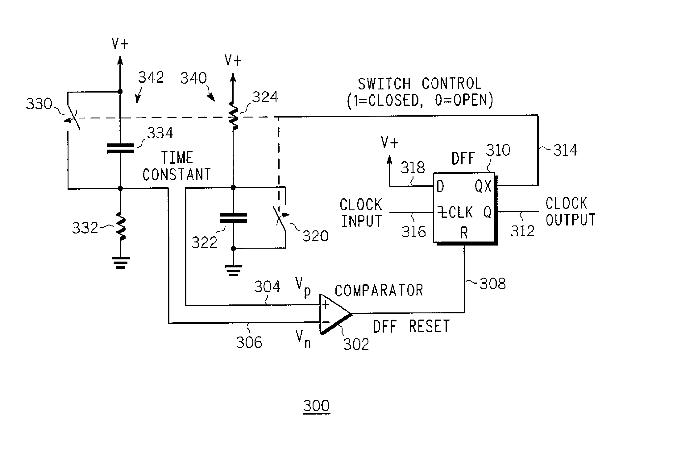
[0013]FIG. 1 illustrates a wireless receiver circuit 100 incorporating a continuous time sigma / delta analog-to-digital converter, in accordance with one embodiment of the present invention. The wireless receiver circuit 100 is a wireless processing circuit that includes an antenna 102 that provides received RF signals to a receiver 104. The receiver 104 of one embodiment is a wireless signal processor that processes a wireless signal by downconverting and conditioning selected received signals in preparation for analog to digital conversion. The receiver 104 provides a downconverted signal 120 to an analog-to-digital (A / D) converter 106. The analog-to-digital converter 106 of one embodiment of the present invention is a continuous time sigma / delta analog-to-digital converter, as is described in detail below. The analog-to-digital converter 106 provides a digitized output signal 122, which represents the selected received signals, to a digital signal processor 108.
[0014]The digital s...
PUM
 Abstract
Description
Claims
Application Information
 - R&D
- Intellectual Property
- Life Sciences
- Materials
- Tech Scout
- Unparalleled Data Quality
- Higher Quality Content
- 60% Fewer Hallucinations
Browse by: Latest US Patents, China's latest patents, Technical Efficacy Thesaurus, Application Domain, Technology Topic, Popular Technical Reports.
© 2025 PatSnap. All rights reserved.Legal|Privacy policy|Modern Slavery Act Transparency Statement|Sitemap|About US| Contact US: help@patsnap.com