
Apparatus for treating wafer

a technology for treating apparatus and wafers, which is applied in the direction of cleaning process and apparatus, cleaning using liquids, chemistry apparatus and processes, etc. it can solve the problems of reducing the effectiveness of cleaning process, batch cleaning apparatus may not remove impurities between minute patterns formed on the wafers, and the time required for cleaning process can be shortened, so as to achieve the effect of sacrificing effectiveness

Inactive Publication Date: 2008-06-17
SAMSUNG ELECTRONICS CO LTD
View PDF15 Cites 0 Cited by
  • Summary
  • Abstract
  • Description
  • Claims
  • Application Information

AI Technical Summary

Benefits of technology

The apparatus achieves uniform ultrasonic oscillation across the wafer surface, improving cleaning effectiveness and reducing processing time while minimizing pattern damage and contamination, allowing for efficient cleaning of multiple wafers simultaneously.

Problems solved by technology

Unfortunately, when a plurality of wafers is simultaneously cleaned using the batch cleaning apparatus, impurities removed from the plurality of wafers may not be drained from the cleaning bath.
The impurities remaining in the cleaning bath may attach to the wafer, thereby reducing the effectiveness of the cleaning process.
In addition, the batch cleaning apparatus may not remove the impurities between the minute patterns formed on the wafer.
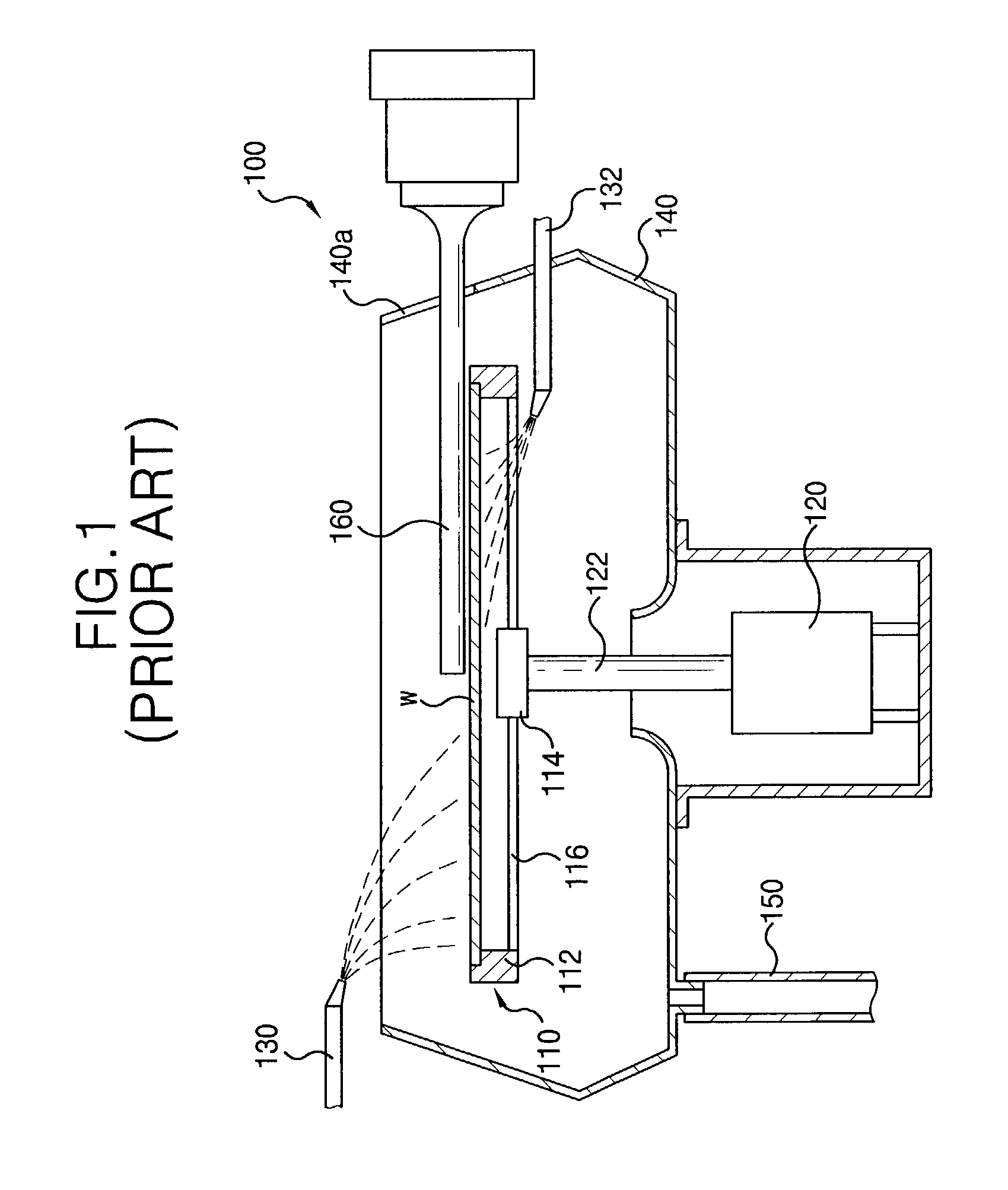
Unfortunately, the elongated rod-shaped quartz probes 160 of the apparatus 100 are frequently broken due to the ultrasonic oscillation.
These quartz probes 160 therefore should not be lengthened beyond a certain length, and as a result, cannot be used effectively for large wafers.
In addition, the amount of ultrasonic oscillation provided by the quartz probe 160 varies depending on the flow rate of the cleaning solution and the rotation speed of the wafer W. The ultrasonic oscillation may therefore not be uniformly applied to the cleaning solution provided on the wafer.
Also, the minute patterns formed on the wafer W may be damaged due to the ultrasonic oscillation applied directly to the cleaning solution on the wafer W.

Method used


Image

  • Apparatus for treating wafer
  • Apparatus for treating wafer
  • Apparatus for treating wafer

Examples


Embodiment Construction

[0035]Various embodiments of the present invention will now be described in detail with reference to the accompanying drawings. It should be noted, however, that the following embodiments are provided by way of example and not of limitation. Various modifications and alterations to the described embodiments will be readily apparent to those of ordinary skill in the art and are therefore considered within the scope of the present invention.

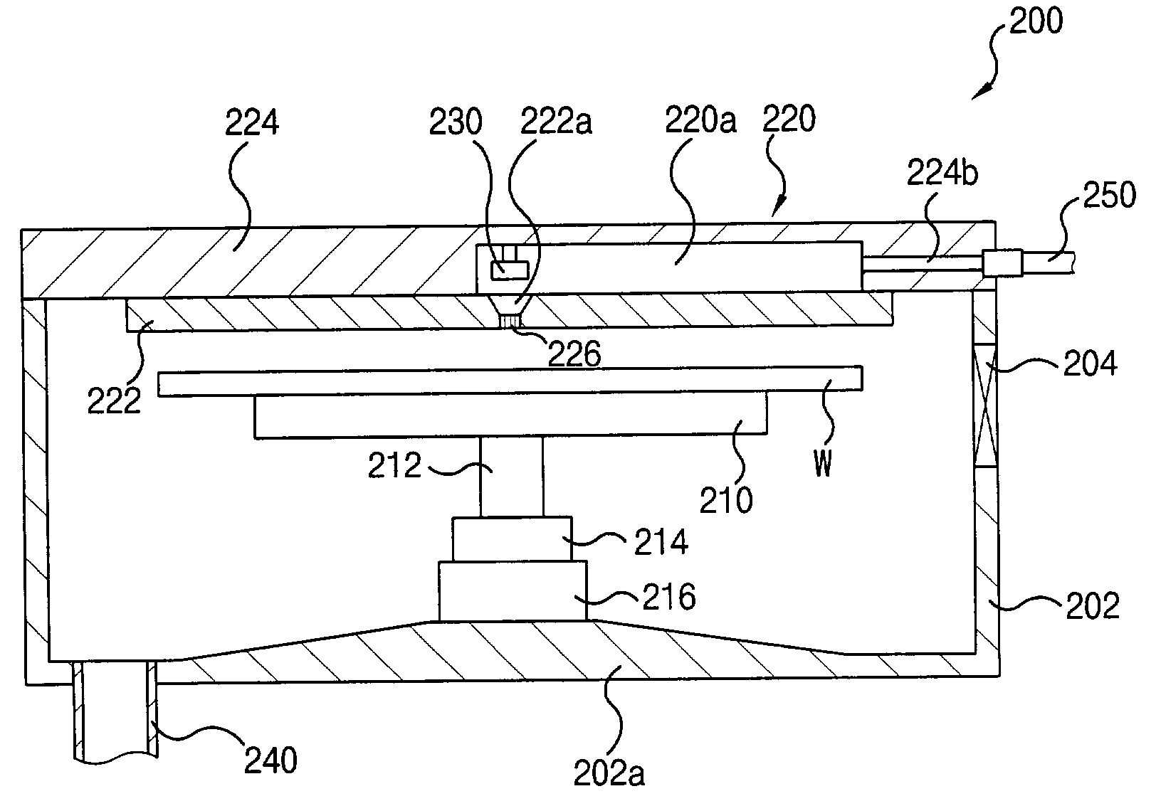
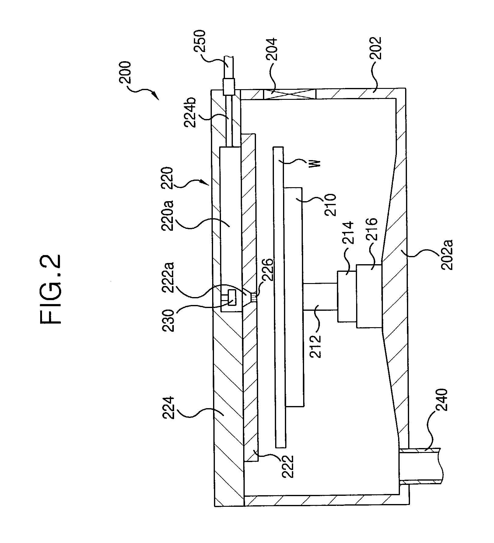
[0036]FIG. 2 is a schematic cross-sectional view of an apparatus 200 for treating a wafer W according to one embodiment of the present invention. Referring to FIG. 2, a wafer treating apparatus 200 has a rotating chuck 210, a treating fluid supplying part 220, an ultrasonic oscillating part 230, and a treating chamber 202. The rotating chuck 210 supports and rotates the wafer W. The rotating chuck 210 can hold the wafer W using any one or more of various methods well known in the art, and a description of the methods for holding the wafer W on the ...


PUM


Abstract

An apparatus for treating a wafer preferably includes a rotating chuck for rotating the wafer and a treating fluid supplying part for supplying the wafer with one or more treating fluids. The treating fluid(s) can be used to clean and / or dry the wafer. The treating fluid supplying part preferably includes a receiving portion for receiving a treating fluid, and a slit communicating with the receiving portion for applying the treating fluid to a surface of the wafer. An ultrasonic oscillating part can be installed in the receiving portion and can apply ultrasonic oscillation to the treating fluid. The treating fluid for applying the ultrasonic oscillation is preferably provided uniformly across the treated surface of the wafer. The effectiveness of the cleaning process can thereby be improved, and damage to patterns formed on the wafer can be reduced.

Description

BACKGROUND OF THE INVENTION[0001]1. Field of the Invention[0002]The present invention relates generally to an apparatus for treating a wafer. More particularly, this invention relates to an apparatus that can clean a wafer by applying a cleaning solution with ultrasonic oscillation and that can dry the wafer using a drying gas.[0003]2. Description of the Related Art[0004]Generally, a semiconductor device is manufactured by repeatedly performing a series of processes on a semiconductor wafer. These processes can include, for instance, a film deposition process, a photolithography process, an etching process, an ion implanting process, a polishing process, a cleaning process, and a drying process. The cleaning and the drying processes are typically performed to remove impurities or undesired films attached to the wafer and to dry the wafer during the other manufacturing processes. The cleaning and drying processes are becoming more important as the patterns formed on the wafer are bec...

Claims


Application Information

Patent Timeline
Patent Type & Authority Patents(United States)
IPC IPC(8): B08B3/00H01L21/304B08B3/12H01L21/00
CPCB08B3/12H01L21/67051Y10S134/902H01L21/304
Inventor PARK
Owner SAMSUNG ELECTRONICS CO LTD
Learn More