Techniques for calibrating on-chip termination impedances

Inactive Publication Date: 2008-05-13
ALTERA CORP
View PDF21 Cites 37 Cited by
  • Summary
  • Abstract
  • Description
  • Claims
  • Application Information

AI Technical Summary

Benefits of technology

[0007]The feedback loop generates calibration control signals for controlling the conductive states of the transistors in the first resistor network. The feedback loop adjusts the calibration control signals to mai

Problems solved by technology

The reflected signal can interfere with the transmitted signal, causing distortion and degrading signal integrity.
However, many integrated circuit packages require a large number of termination resistors, because they have a large number of I / O pins.
However, the impedance of on-chip resistors varies as the temperature of the integrated circuit changes.
When the impedance of an on-chip termination circuit is not equal to the characteristic impedance of the transmission line, signal reflection typically increases, causing increased signal distortion.
However, many prior art on-chip termination calibration circuits do not provide a high enough accuracy for some applications.

Method used


Image

  • Techniques for calibrating on-chip termination impedances
  • Techniques for calibrating on-chip termination impedances
  • Techniques for calibrating on-chip termination impedances

Examples


Embodiment Construction

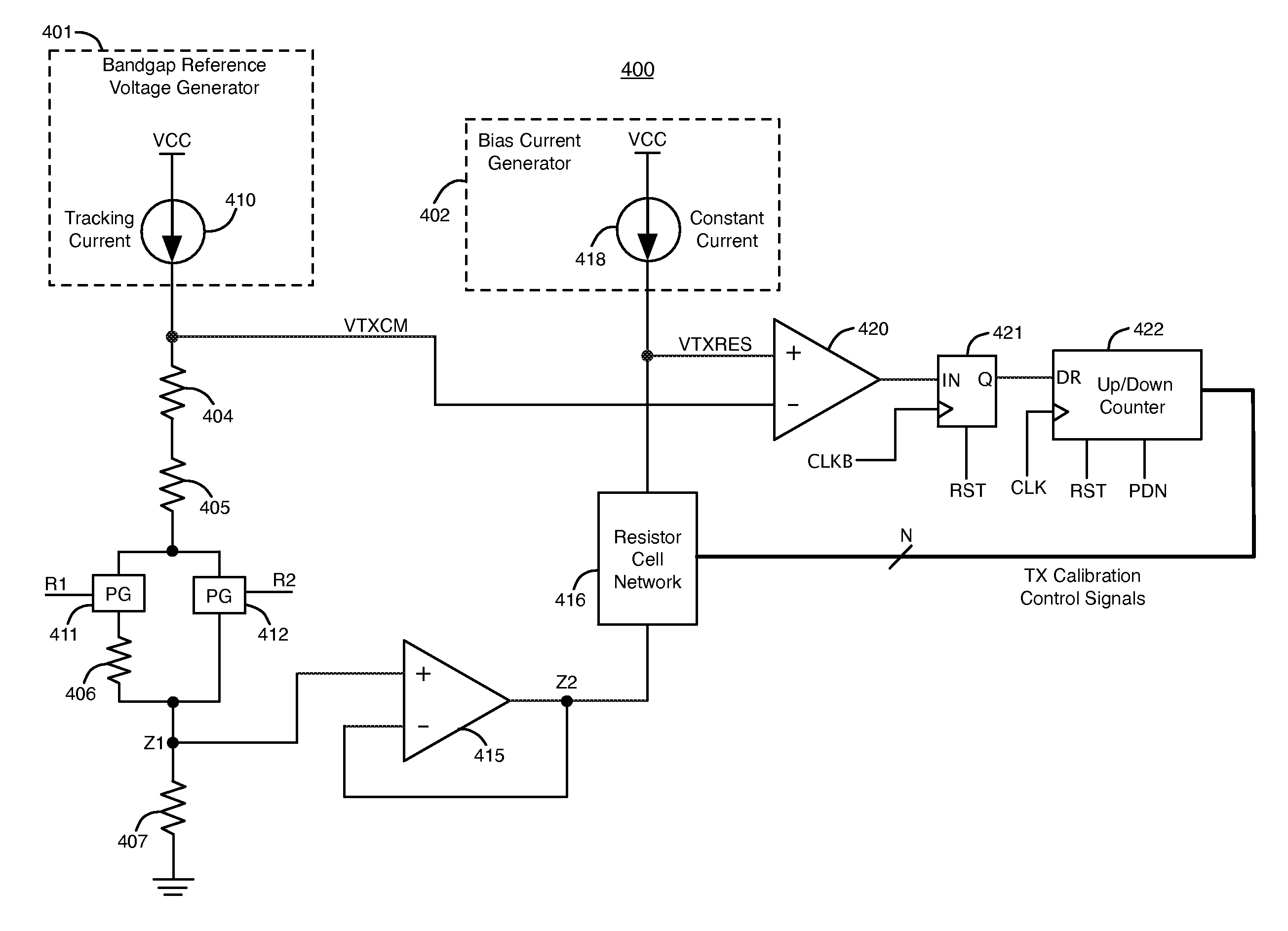
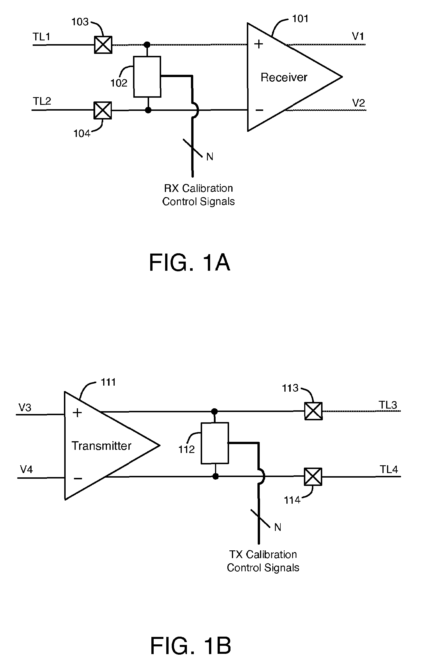
[0019]FIG. 1A illustrates a receiver buffer 101 and a receiver on-chip termination (OCT) circuit 102, according to an embodiment of the present invention. Receiver buffer 101 and receiver OCT circuit 102 are located on an integrated circuit die. Differential signals are transmitted from a transmitter (not shown) through transmission lines TL1 and TL2 to differential input pins 103 and 104, respectively. Receiver 101 has plus and minus inputs that are coupled to pins 103 and 104, respectively, to receive the differential input signals from transmission lines TL1 and TL2. Receiver 101 generates differential output signals V1 and V2.

[0020]Receiver OCT circuit 102 is coupled between pins 103 and 104. OCT circuit 102 provides a matching termination impedance to transmission lines TL1 and TL2 to prevent signal reflection from receiver 101. OCT circuit 102 includes one or more resistors and one or more pass gates. An N number of receiver (RX) calibration control signals control the conduct...


PUM


Abstract

A calibration circuit block includes a first resistor network, a second resistor network, and a feedback loop. The first resistor network includes a set of transistors and receives a constant current from a constant current source. The second resistor network receives a tracking current from a tracking current source. The impedance of the second resistor network changes with temperature and process variations on the integrated circuit. The tracking current source compensates for variations in the impedance of the second resistor network that are caused by process and temperature variations to maintain a constant reference voltage at the second resistor network. The feedback loop generates calibration control signals for controlling the conductive states of the transistors in the first resistor network. The feedback loop adjusts the calibration control signals to maintain a constant impedance in the first resistor network.

Description

BACKGROUND OF THE INVENTION[0001]The present invention relates to electronic circuits, and more particularly, to techniques for calibrating on-chip termination impedances for transmitters and receivers to terminate transmission lines.[0002]Signal reflection can occur on transmission lines when there is a mismatch between the characteristic impedance of the transmission line and the impedance of the transmitter and / or receiver. The reflected signal can interfere with the transmitted signal, causing distortion and degrading signal integrity.[0003]To solve this problem, transmission lines are resistively terminated by a matching impedance to minimize or eliminate signal reflection. Input / output (I / O) pins on an integrated circuit package can be terminated by coupling external termination resistors to the appropriate I / O pins. However, many integrated circuit packages require a large number of termination resistors, because they have a large number of I / O pins. Therefore, it is becoming...

Claims


Application Information

Patent Timeline
IPC IPC(8): H03K19/003
CPCH04L25/0278H04L25/0272H04L25/0292G11C29/022G11C29/025G11C29/028
Inventor WEI, KWONG-WEN
Owner ALTERA CORP
Why Eureka
Try Eureka