Constant impedance driver for high speed interface

a driver and high-speed technology, applied in logic circuit coupling/interface arrangement, pulse technique, baseband system details, etc., can solve the problems of lrc load, memory card system frequently present complex inductive/resistive/capacitive load, etc., and achieve constant impedance and constant impedance

Inactive Publication Date: 2002-11-07
GLOBALFOUNDRIES US INC
View PDF0 Cites 8 Cited by
  • Summary
  • Abstract
  • Description
  • Claims
  • Application Information

AI Technical Summary

Benefits of technology

0020] In a further aspect, the present invention provides, in an integrated circuit, a method of maintaining a desired output impedance of an off-chip driver circuit having an off-chip driver device despite variations in operating conditions. The method comprises generating a variable level control signal using a sample driver device being a scaled representative of the off-chip driver device. The control signal varies in level according to variable operating conditions presented to the sample driver device, with the variable operating conditions also being presented to the off-chip driver device. The method further includes applying the variable level control signal to the off-chip driver device to control output impedance of the off-chip driver circuit. Desired output impedance of the off-chip driver circuit is maintained despite variation in the variable operating conditions.
0021] The generating step may further comprise comparing a voltage obtained from operating the sample driver device to a reference voltage, and supplying the sample driver device with constant current. Such constant current may be supplied to the sample device through a sample resistance scaled and representative of resistance in the off-chip driver device.
0022] In yet another aspect, the present invention is directed to a method of compensating a driver for maintaining constant impedance during data transfer from an integrated circuit. The method comprises providing an output portion having an output device adapted to transfer data from the integrated circuit, and generating a reference voltage. A reference current is accepted and there is generated a sample voltage in a mimic circuit portion having a sample output device scaled to a fraction of the output device. A control voltage is generated in a differential amplifier portion in response to the reference voltage and the sample voltage. The method also includes switching either the control voltage, a power supply voltage or ground to the output stage in response to a data input, the control voltage regulating the output device in the output stage portion to achieve a more constant impedance.
0023] Preferably, the reference voltage is generated by a voltage divider circuit. The method may further include changing the reference current or the reference voltage to change the output portion to a different, constant impedance. The output device of the output portion preferably comprises a multiple of the sample output device of the mimic circuit portion. In the preferred embodiment, the differential amplifier develops an error voltage and apply it to the control voltage to cause the mimic circuit portion and the differential amplifier portion to reach equilibrium.
0024] The reference current may be a constant current, and the method may further include providing a sample resistance in the mimic circuit portion scaled and representative of resistance in the output portion, such that the constant current flows through the sample resistance.
0025] The output portion may include an NFET output device such that the switching step applies either the ground or the predetermined control voltage to the NFET output device. In another embodiment, the output portion may include a PFET output device such that the switching step applies either a power supply voltage or the predetermined control voltage to the PFET output device.

Problems solved by technology

Variable impedance of a driver will cause reflections and data integrity problems.
Memory card systems frequently present a complex inductive / resistive / capacitive (LRC) load with transmission line reflections resulting from multiple dynamic random access memory (DRAM) slots on a single data trace.

Method used


Image

  • Constant impedance driver for high speed interface
  • Constant impedance driver for high speed interface
  • Constant impedance driver for high speed interface

Examples


Embodiment Construction

)

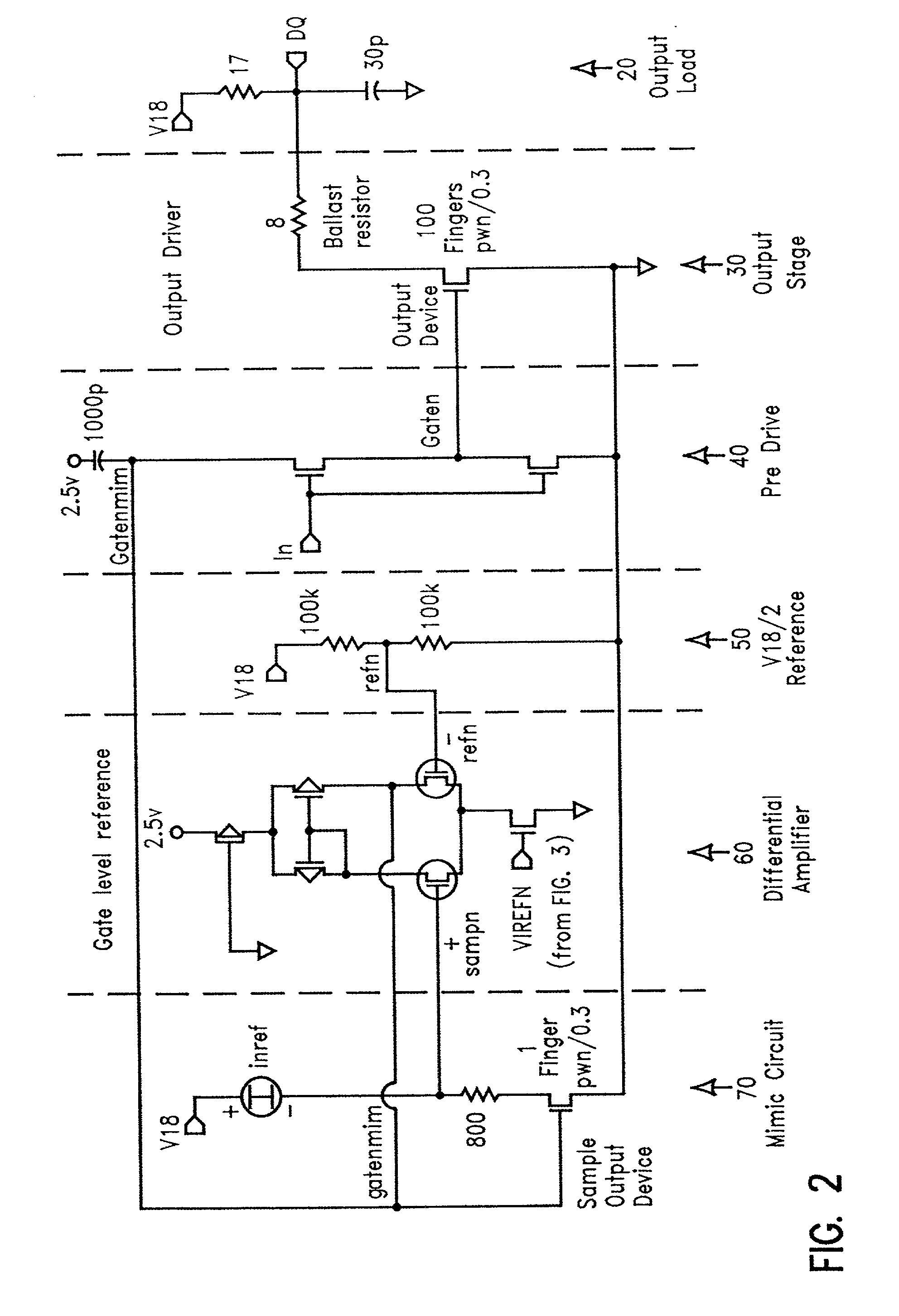
[0034] In describing the preferred embodiment of the present invention, reference will be made herein to FIGS. 1-6 of the drawings in which like numerals refer to like features of the invention. Features of the invention are not necessarily shown to scale in the drawings.

[0035] The present invention provides a circuit in which the impedance of a driver changes depending on what processing the chip received due to variations in PVT, i.e., processing tolerance, the voltage at which the chip is run, and the temperature of the chip. A non-limiting example of the present invention is as a constant impedance dynamic random access memory (DRAM) driver for a high speed memory interface.

[0036] Referring to FIG. 2, the preferred embodiment of the present invention is shown coupled to output load portion 20, output stage portion 30, predrive stage portion 40, reference portion 50, differential amplifier portion 60, and mimic circuit portion 70. The driver of the present invention is controlle...


PUM


Abstract

A compensated driver for maintaining constant impedance during data transfer from an integrated circuit comprises an output portion having an output device to transfer data from the integrated circuit and a mimic circuit portion having a sample output device scaled to a fraction of the output device adapted to accept a reference current and generate a sample voltage. A mimic circuit portion has a sample output device scaled to a fraction of the output device adapted to accept a reference current and generate a sample voltage. A differential amplifier portion is adapted to generate a control voltage in response to a reference voltage and the sample voltage A predrive portion applies either a ground or the predetermined control voltage from the differential amplifier portion to the output stage portion in response to an input, the control voltage regulating the output device in the output stage portion to achieve a more constant impedance

Description

[0001] 1. Field of the Invention[0002] The present invention relates to integrated circuit technology and, in particular, to a constant impedance driver for a high speed interface.[0003] 2. Description of Related Art[0004] Off-chip drivers are needed to output data, e.g., an address or a logic result, from one integrated circuit (IC) chip and transfer it to another IC chip. Such data is driven through circuitry in various types of devices, such as an IC package, a printed circuit board, or simply wires or cables. Off-chip drivers act as an interface between the output of one IC chip to become input of another IC chip. The most efficient transfer of data is achieved if one knows the interconnecting wiring and load, and designs the off-chip driver to match that impedance. Variable impedance of a driver will cause reflections and data integrity problems.[0005] Memory card systems frequently present a complex inductive / resistive / capacitive (LRC) load with transmission line reflections r...

Claims


Application Information

Patent Timeline
Patent Type & Authority Applications(United States)
IPC IPC(8): H03K19/003H04L25/02
CPCH03K19/00384H04L25/028H04L25/0278
Inventor FIFIELD, JOHN A.HOUGHTON, RUSSELL J.
Owner GLOBALFOUNDRIES US INC
Why Eureka
Try Eureka