
Hardmask for reliability of silicon based dielectrics

a silicon-based dielectric and reliability technology, applied in the field of integrated circuits, can solve the problems of poor quality and reliability, low k dielectric reliability, and prior art reliability problems, and achieve the effects of reliable electrical characteristics, improved reliability, and improved reliability

Active Publication Date: 2008-02-26
GLOBALFOUNDRIES U S INC
View PDF4 Cites 12 Cited by
  • Summary
  • Abstract
  • Description
  • Claims
  • Application Information

AI Technical Summary

Benefits of technology

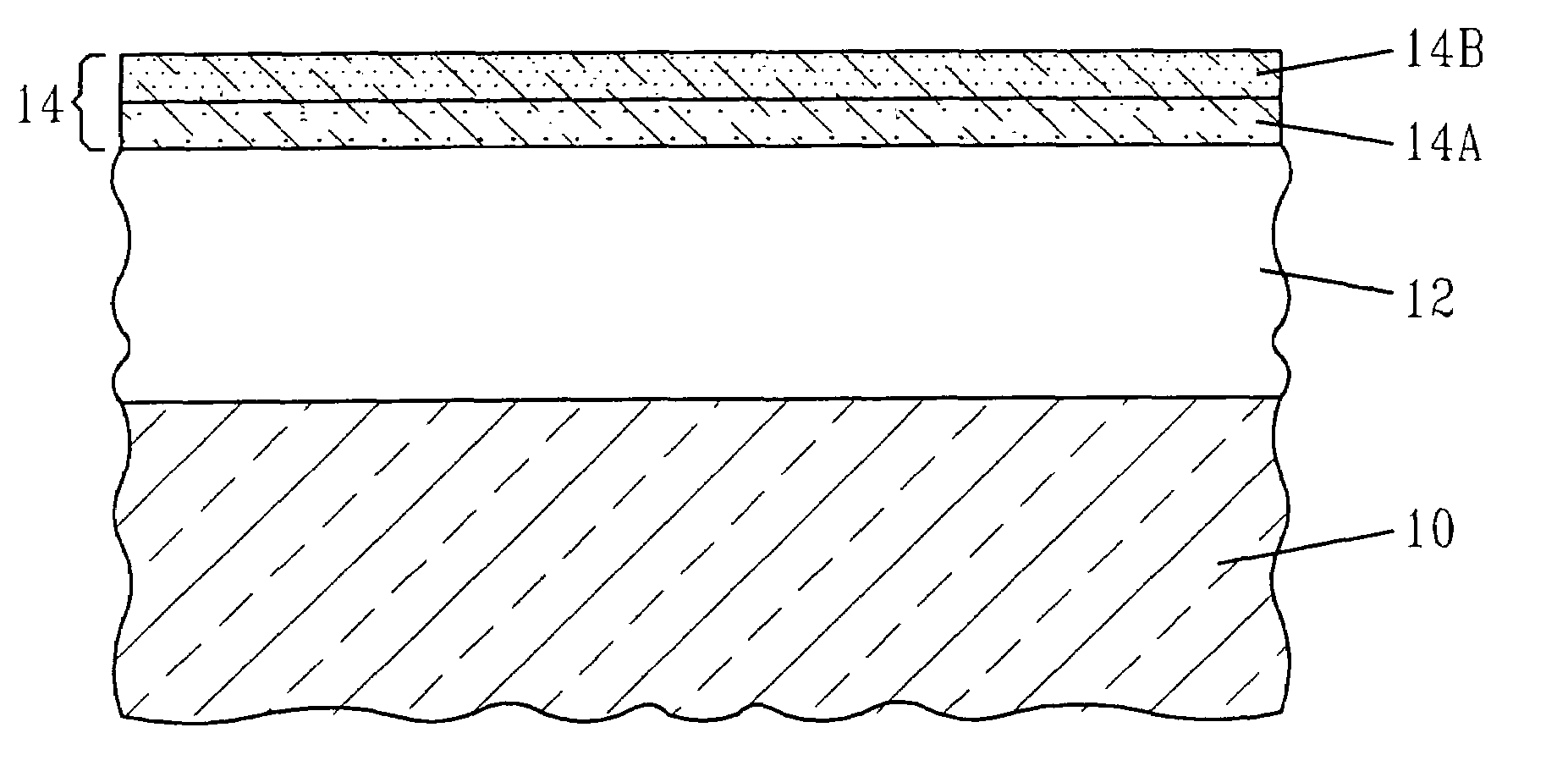
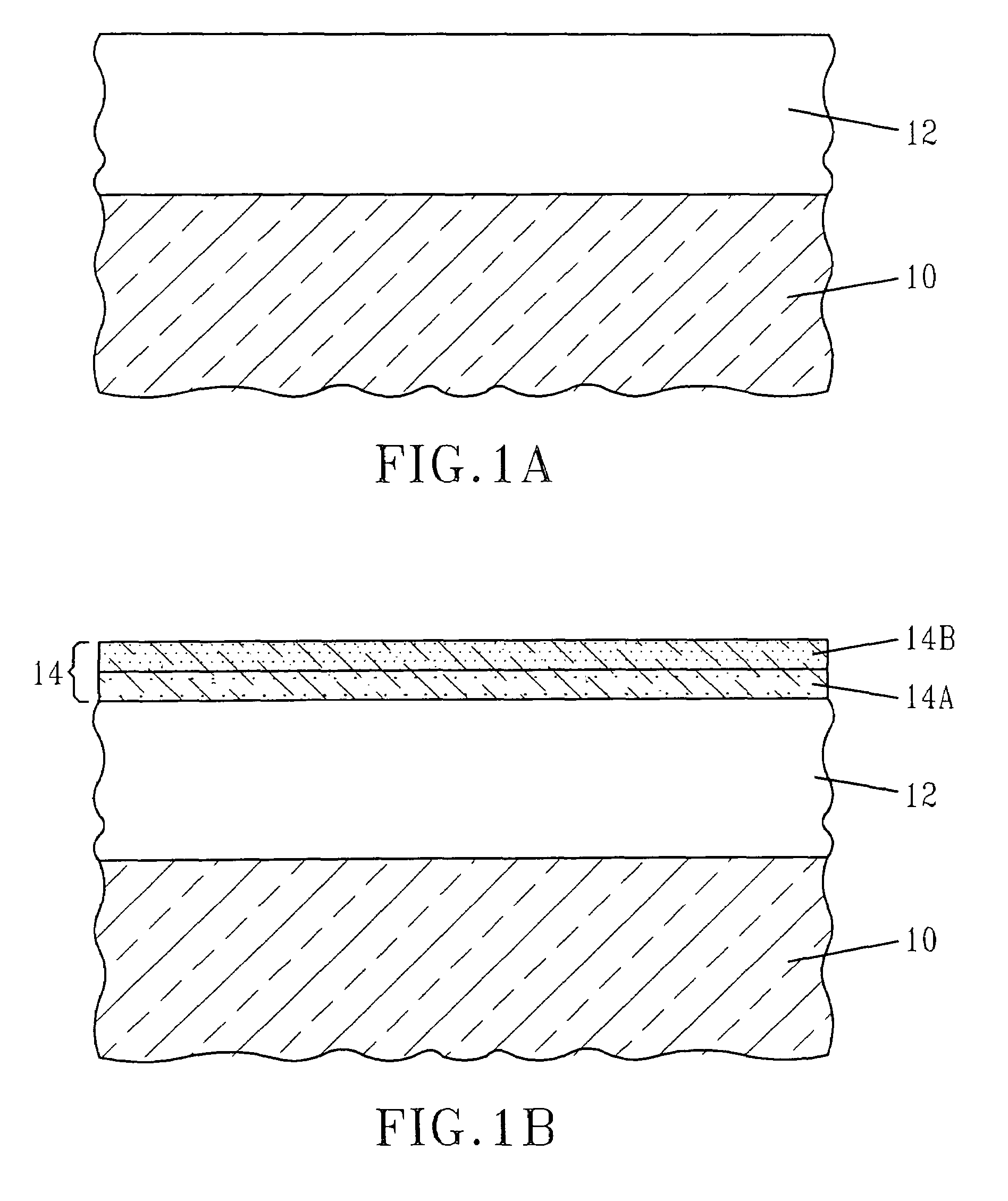
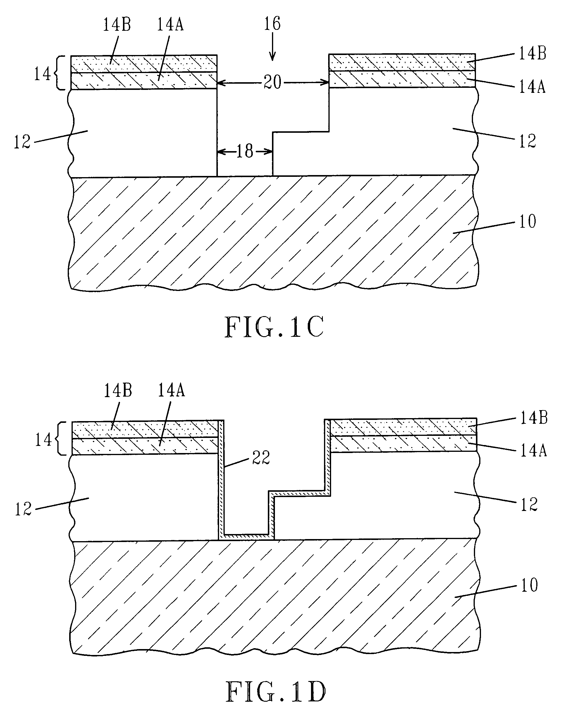
The present invention provides a back-end-of-the-line (BEOL) interconnect structure with improved reliability in a low k dielectric. The structure has stable electrical characteristics and does not show delamination or moisture adsorption that would lead to poor dielectric breakdown. The structure includes an improved hardmask with a graded composition that acts as a moisture barrier and a chemical mechanical polishing (CMP) etch stop layer. The hardmask is located on a surface of the low k dielectric material and has at least one opening in which a liner and conductive material are formed. The invention also provides a method for fabricating the hardmask in a simplified process.

Problems solved by technology

However, reliability problems are associated with these prior art structures.
During integration, reliability stress, or extended use, a chip interconnect structure made in a low k dielectric may fail or degrade due to poor adhesion, moisture uptake, and various stress migration between the metal liner / metal and the low k dielectric.
This poor quality and reliability results from the defects in the low k dielectric film and the metal liner, allowing metal or metal ions, e.g., Cu or Cu ions, to penetrate the dielectric allowing oxidizing species such as H2O or O2 to interact with the metal.
The problems become serve with the introduction of porous low k films where nanopores are present in the film to reduce the dielectric constant of the same.
The mechanical properties of these porous low k films are less robust as compared to a conventional SiO2 dielectric for subsequent device fabrication and packaging.
As a result, significant interlevel dielectric film cracking may occur as the low k dielectric film becomes more porous, especially when it is exposed to moisture.
Moreover, the effective cohesive strength of porous low k films is reduced, as the dielectric film is prone to stress cracking.
In an integrated structure and when a blanket dielectric layer is deposited over an underlying patterned layer, the driving force for cracking increases due to the thermal mismatch between the metal interconnect lines and the dielectric.
As a result, cracking may occur in the overlying blanket dielectric film even though the film itself does not contain enough driving force to induce cracking.
In view of the above, there is a need to prevent moisture absorption, reduce cracking and improve mechanical properties of low k dielectric films and to enhance the reliability of the metal / low k dielectric interconnect faces by reducing the defect of the low k dielectrics that are caused by open pores and result in easy moisture adsorption during subsequent processing steps, poor adhesion between interfaces, increased cracking force and ultimately failed device reliability.

Method used


Image

  • Hardmask for reliability of silicon based dielectrics
  • Hardmask for reliability of silicon based dielectrics
  • Hardmask for reliability of silicon based dielectrics

Examples


example

[0081]In this example, four different OMCATS-containing hardmasks (HMs) of the present invention were made by PECVD using the conditions in the following table.

[0082]

TABLEOMCATSOMCATSOMCATSOMCATSHM 1HM 2HM 3HM 4300 mm300 mm300 mm200 mm*OMCATS Flow (mgm)2000250028001800O2 Flow (sccm)01602200He Carrier100010001000500Flow (sccm)Temp. (° C.)350350350350Pressure (Torr)5555Spacing (mils)450450450450HF power (W)500500400500LF power (W)01506075*For OMCATS HM 4 prepare in 200 mm Plasma CVD system (Column 5), typical electrical breakdown plots, breakdown plot and J-E plot are shown in FIGS. 2A and 2B. It can be seen from the plots that this film had excellent breakdown properties of 8 MV / cm and a low electrical leakage of less than 2 × 10E−9 A / cm2 at 2 MV / cm.

[0083]The FTIR spectrum shown in FIG. 3 reveals a typical plasma SiCOH film structure with stable Si—O, Si—CH3, Si—H and cross-linking Si—CH2—Si bonding in the film. The typical Auger Profile (FIG. 4) of SiCOH film without O2 precursor sh...


PUM

PropertyMeasurementUnit
dielectric constantaaaaaaaaaa
densityaaaaaaaaaa
densityaaaaaaaaaa

Abstract

The present invention provides a hardmask that is located on a surface of a low k dielectric material having at least one conductive feature embedded therein. The hardmask includes a lower region of a hermetic oxide material located adjacent to the low k dielectric material and an upper region comprising atoms of Si, C and H located above the hermetic oxide material. The present invention also provides a method of fabricating the inventive hardmask as well as a method to form an interconnect structure containing the same.

Description

DESCRIPTION[0001]1. Field of the Invention[0002]The present invention generally relates to integrated circuits (ICs), and more particularly to silicon based dielectrics using interconnect structures, including multilevel interconnect structures fabricated by damascene methods, in which the dielectric is a low k dielectric having a dielectric constant of about 3.0 or less. The present invention describes improved reliability of silicon based dielectrics as well as interconnect structures containing metal wiring such as copper within these low k dielectrics, the structures are improved by introducing a dense, graded hardmask on top of each of the silicon based dielectrics. The present invention also describes a method to make the inventive hardmask structure as well as a method to use in the inventive hardmask in an interconnect structure.[0003]2. Background of the Invention[0004]Generally, semiconductor devices include a plurality of circuits which form an IC fabricated on a single c...

Claims


Application Information

Patent Timeline
Patent Type & Authority Patents(United States)
IPC IPC(8): H01L23/12
CPCH01L21/02126H01L21/02274H01L21/3122H01L21/3148H01L21/76825H01L21/76826H01L21/76828H01L21/76832H01L23/53295H01L21/02216Y10T428/24802H01L21/76807H01L2924/0002H01L2924/00H01L21/02211
Inventor NGUYEN, SON VANLANE, MICHAELGATES, STEPHEN M.LIU, XIAO H.MCGAHAY, VINCENT J.MEHTA, SANJAY C.SHAW, THOMAS M.
Owner GLOBALFOUNDRIES U S INC
Learn More