Exposure apparatus

a technology of exposure apparatus and chuck, which is applied in the field of exposure apparatus, can solve the problems of reducing the reflectance of euv light, temperature rise in the chuck, and the device such as the reticle or the wafer cannot be flat, and achieves excellent throughput and optical performance, reduce the fraction of defective wafers, and poor response to position control

Inactive Publication Date: 2008-02-05
CANON KK
View PDF15 Cites 3 Cited by
  • Summary
  • Abstract
  • Description
  • Claims
  • Application Information

AI Technical Summary

Benefits of technology

[0021]Accordingly, it is an exemplary object to provide an exposure apparatus with excellent throughput and optical performance, which can cool the object (for example, optical elements such as the wafer or the reticle) effectively without causing worse vibrations, position instability, and / or poor responses to position control; while reducing the fraction of defective wafers by precisely exposing the circuit pattern, and fabricating a high quality device.
[0022]Another exemplary object is to provide an exposure apparatus which can cool both the object and the object holder effectively, reduce the fraction of defective wafers by exposing the circuit pattern more precisely, and fabricate a higher quality device.
[0023]Still another exemplary object is to provide an exposure apparatus which can detect the temperature of the object surface easily and the temperature of the holding member precisely, reduce the fraction of defective wafers by exposing the circuit pattern more precisely, and fabricate a higher quality device.

Problems solved by technology

This causes a problem by decreasing the reflectance of the EUV light due to absorption by the adhered carbon.
A leakage current among the electrodes running in the chuck generates heat and causes a temperature rise in the chuck.
In holding the device on the chuck, a device such as the reticle or the wafer cannot be flat when a particle is wedged between these devices and the chuck because the precision of the projection exposure decreases.
However, the chuck used in the EUV exposure apparatus cannot use materials having an ideal low coefficient of thermal expansion because it should keep sufficient electrostatic suction force.
A position shift of 4.5 nm by thermal expansion may be a problem because the demand for position accuracy of the wafer chuck in the EUV exposure apparatus is less than a few nanometers.
However, friction suctions between the wafer and the chuck surface restricts thermal expansion.
For example, a temperature rise of 1 degree centigrade in the reticle causes a problem with a thermal expansion of approximately 5 nm.
The heat expansion of the optical elements, such as the wafer and the chuck, due to the temperature rise makes transfer of the circuit pattern in exposure imprecise.
As the optical element and the chuck are arranged in vacuum state, it is difficult to apply a cooling method using heat transfer by convection in the EUV exposure apparatus.
However, a precision stage such as the wafer stage for supporting the wafer chuck or the reticle stage for supporting the reticle chuck is supported by an elastic element with low rigidity (for example, a spring).
Therefore, with the flow of liquid coolant in the optical element or the chuck, the position of the wafer or the reticle becomes unstable because of vibrations caused by the swirls and / or pulsations generated in the flow paths or pipes.
Because the pipe, which is connected to the optical element or the chuck, restricts movement of the precision stage; the position detection and position control responses to the precision stage using an interferometer decreases, and the control for lowering high frequency vibration becomes difficult.
In cases where a pin chuck is used, heat transfer between the pin chuck and the optical element is difficult because the contact area of the pin and the optical element is small.
Therefore, there is an optical element cooling problem on the one hand and using the chuck to cool effectively on the other.
The problem will be more serious if the contact area of the pin and the optical element is 10% or smaller than the area of the optical element.
Impartial cooling of heat generated in the circuit board of the optical element or the chuck causes fluctuation in heat expansion despite a decrease in the heat, resulting in precise positioning difficulties of the optical elements, such as the wafer or the reticle.

Method used


Image

  • Exposure apparatus
  • Exposure apparatus
  • Exposure apparatus

Examples


first embodiment

[0040][The First Embodiment]

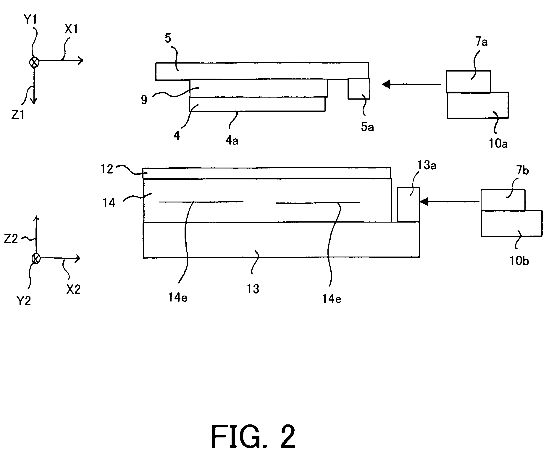
[0041]Referring now to the accompanying drawings, a description will now be given of an exposure apparatus of the first embodiment according to the present invention. FIG. 1 is a schematic structure of the whole exposure portion in an exposure apparatus 1 of the first embodiment according to the present invention. The exposure apparatus 1 is a scanning type reduction projection exposure apparatus using EUV light 2e as exposure light. It includes an EUV light source 2 for emitting EUV light 2e, an illumination system 3, a reflection reticle as an object (hereinafter “reticle”) 4, a reticle stage 5, a projection optical system 6, a laser interferometer for the reticle 7a and for the wafer 7b as a position measuring device (see FIG. 2), an alignment detector 15, a focus position detector 16, and a vacuum system 17.

[0042]The EUV light source uses, for example, a laser plasma light source 2a. The laser plasma light source 2a has a pulse laser 2b for excitation...

second embodiment

[0076][The Second Embodiment]

[0077]Referring now to FIG. 6, a description will now be given of an exposure apparatus of the second embodiment according to the present invention. FIG. 6 is an enlarged view around the wafer 12 and a wafer chuck 14 in an exposure apparatus 1 of the second embodiment. The same structure described in the first embodiment is designated by the same reference numeral, and a description will be omitted.

[0078]A temperature controller 18 for the substrate controls the temperature of the refrigerator 11a used to control the temperature of the wafer 12. A non-contact type radiation heat transfer sensor (a first sensor) 19 connects to the temperature controller 18 for the substrate. The radiation heat transfer sensor 19 detects the surface temperature of the wafer 12 without contacting it, while the temperature controller 18 for the substrate maintains the temperature of the wafer 12 at 23 degree centigrade by adjusting the applied voltage to the Peltier device 1...


PUM

PropertyMeasurementUnit
wavelengthsaaaaaaaaaa
air pressureaaaaaaaaaa

Abstract

An exposure apparatus includes an optical system for guiding light to an object, a holding member for holding the object, a first refrigerator located near a holding side of the holding member without contacting the holding side, and a second refrigerator located near a backside of the holding member without contacting the backside.

Description

[0001]This application claims the right of priority under 35 U.S.C. §119 based on Japanese Patent Application No. 2003-104422 filed on Apr. 8, 2003, which is hereby incorporated by reference herein in its entirety as if fully set forth herein.BACKGROUND OF THE INVENTION[0002]The present invention relates generally to exposure apparatuses for fabricating, for example, semiconductor devices, imaging devices, liquid crystal display devices, thin film magnetic heads, and other micro devices, and more particularly to an exposure apparatus that exposes by using EUV light (extreme ultraviolet light) or X-ray and the like.[0003]Conventionally, reduction projection exposure with UV light have been used for lithography to manufacture fine semiconductor devices like semiconductor memories or logic circuits. The transferable minimum critical dimension in the reduction projection exposure is proportionate to a wavelength of light used for exposure, and inversely proportionate to the numerical ap...

Claims


Application Information

Patent Timeline
Patent Type & Authority Patents(United States)
IPC IPC(8): F25B21/02F25D23/12G03B27/42G03F7/20H01L21/00H01L21/027H10N10/00
CPCF25B21/02G03B27/42G03F7/70708G03F7/70875H01L21/67109H01L21/67248H01L35/00H10N10/00
Inventor HARA, SHINICHI
Owner CANON KK
Why Eureka
Try Eureka