
Electronic assemblies with filled no-flow underfill

a technology of electronic assemblies and underfill, applied in the field of electronic assembly with no-flow underfill, can solve the problems of increasing overall manufacturing costs, increasing the difficulty of obtaining adequate underfill dispersion through capillary forces alone, and increasing the overall manufacturing cos

Inactive Publication Date: 2008-01-29
MICRON TECH INC
View PDF25 Cites 31 Cited by
  • Summary
  • Abstract
  • Description
  • Claims
  • Application Information

AI Technical Summary

Benefits of technology

This approach enhances the reliability and yield of IC packages by reducing thermal expansion mismatch and particle interference, resulting in improved electrical and mechanical contact and reduced manufacturing costs.

Problems solved by technology

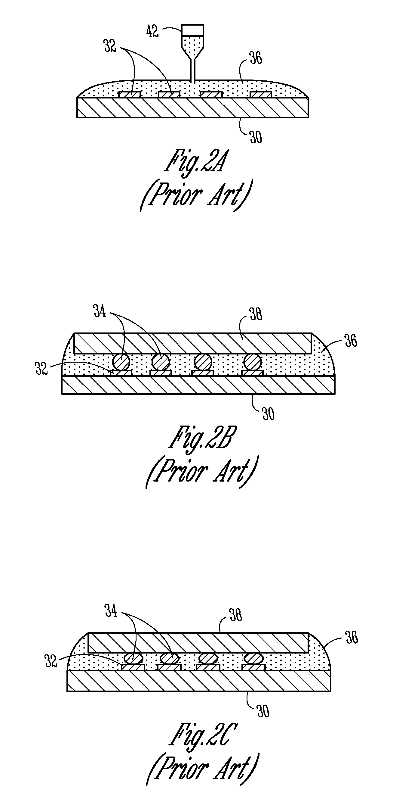
However, this method requires separate operations to perform solder reflow, dispense the underfill, clean up any excess underfill, facilitate underfill capillary flow, and perform underfill cure, thus increasing the overall manufacturing costs.
Also, with the die bump pitch and bump height decreasing and terminal count increasing, it becomes successively more difficult to obtain adequate underfill dispersion through capillary forces alone.
High performance ICs generate sufficient heat and may also be exposed to sufficient ambient heat to cause reliability problems in the form of cracked bump-to-pad connections, if the coefficient of thermal expansion (CTE) of the underfill material is significantly higher than that of silicon and / or the IC substrate material, e.g. FR-4.
However, adding particles increases the underfill viscosity, making it more difficult to apply through capillary forces.
However, if sufficient particles are added to the underfill to lower its CTE, the particles tend to cause a significant interconnection yield problem, because they get interposed between the IC bumps and the substrate pads and prevent good solder joints.

Method used


Image

  • Electronic assemblies with filled no-flow underfill
  • Electronic assemblies with filled no-flow underfill
  • Electronic assemblies with filled no-flow underfill

Examples


Embodiment Construction

[0017]In the following detailed description of embodiments of the invention, reference is made to the accompanying drawings which form a part hereof, and in which is shown by way of illustration specific preferred embodiments in which the subject matter may be practiced. These embodiments are described in sufficient detail to enable those skilled in the art to practice them, and it is to be understood that other embodiments may be utilized and that structural, mechanical, compositional, procedural, and electrical changes may be made without departing from the spirit and scope of the present subject matter. Such embodiments of the inventive subject matter may be referred to, individually and / or collectively, herein by the term “invention” merely for convenience and without intending to voluntarily limit the scope of this application to any single invention or inventive concept if more than one is in fact disclosed. The following detailed description is, therefore, not to be taken in ...


PUM

PropertyMeasurementUnit
sizeaaaaaaaaaa
soaking temperatureaaaaaaaaaa
pressureaaaaaaaaaa

Abstract

High yield, high reliability, flip-chip integrated circuit (IC) packages are achieved utilizing a combination of heat and pressure to bond flip-chip die and to cure no-flow underfill material. The underfill comprises a filler or low coefficient of thermal expansion (CTE) material to decrease CTE of the cured underfill. The filler material can be selected from the group comprising silica, silicon oxide, silicon dioxide, silicon nitride, aluminum oxide, aluminum nitride, or a mixture thereof. The filler material may also increase the viscosity of the uncured underfill and / or increase the modulus of elasticity of the cured underfill. In some method embodiments, a thermocompression bonder is used to simultaneously provide solder bump reflow and underfill curing. Application of various methods to a component package, an electronic assembly, and an electronic system are also described.

Description

TECHNICAL FIELD [0001]The present subject matter relates generally to electronics packaging. More particularly, the present subject matter relates to an electronic assembly that includes a component package, such as an integrated circuit (IC) package, comprising a filled no-flow underfill material to increase yield and reliability, and to manufacturing methods related thereto.BACKGROUND INFORMATION[0002]Electronic components, such as integrated circuits (ICs), are typically assembled into component packages by physically and electrically coupling them to a substrate made of organic or ceramic material. One or more component packages, such as IC packages, can be physically and electrically coupled to a printed circuit board (PCB) to form an “electronic assembly”. The “electronic assembly” can be part of an “electronic system”. An “electronic system” is broadly defined herein as any product comprising an “electronic assembly”. Examples of electronic systems include computers (e.g., de...

Claims


Application Information

Patent Timeline
Patent Type & Authority Patents(United States)
IPC IPC(8): H01L21/00H01L21/44H01L29/40H01L21/56
CPCH01L21/563H01L24/29H01L24/32Y10T29/49146H01L2224/73203H01L2224/73204H01L2224/83192H01L2924/01005H01L2924/01013H01L2924/01015H01L2924/01029H01L2924/01033H01L2924/01075H01L2924/01079H01L2924/01082H01L2924/14H01L2924/1433H01L2924/3511H01L2224/32225H01L2924/01006H01L2924/01087H01L2224/16225Y10T29/49144H01L2924/00011H01L2224/325H01L2224/29386H01L2224/2929H01L2224/29036H01L2224/81903H01L2224/81193H01L2924/10253H01L2924/00H01L2924/3512H01L2924/05442H01L2924/00012H01L2224/29075H01L2924/12044
Inventor GONZALEZ, CARLOS A.SHI, SONG-HUADJUKIC, MILAN
Owner MICRON TECH INC
Learn More