
Controlling threading dislocation densities in Ge on Si using graded GeSi layers and planarization

a technology of gesi layer and planarization, applied in the direction of light-sensitive devices, capacitors, electrolytic capacitors, etc., can solve the problems of dislocation pile-up, three-dimensional misfit dislocation network, and dislocation dislocation,

Inactive Publication Date: 2007-07-31
MASSACHUSETTS INST OF TECH
View PDF214 Cites 89 Cited by
  • Summary
  • Abstract
  • Description
  • Claims
  • Application Information

AI Technical Summary

Benefits of technology

This approach effectively reduces threading dislocation density and surface roughness, preventing dislocation pile-ups and cracking, resulting in higher quality semiconductor structures with lower defect densities, suitable for integrating III-V materials on Si substrates.

Problems solved by technology

The relaxed graded buffer introduces a 4% lattice mismatch between Si and Ge gradually, resulting in a disperse, three-dimensional misfit dislocation network.
However, a complication arises during thick grades to high Ge concentrations.
The characteristic crosshatch surface roughness and the underlying strain fields of the misfit array can overlap, blocking threading dislocation glide and leading to dislocation pile-ups.
The formation of these pile-ups necessitates the nucleation of additional threading dislocations, as the trapped threading dislocations can no longer contribute to strain relief.
Growth on off-cut Si substrates has been shown to improve surface morphology and decrease the number of pileups, but not eliminate them entirely.

Method used


Image

  • Controlling threading dislocation densities in Ge on Si using graded GeSi layers and planarization
  • Controlling threading dislocation densities in Ge on Si using graded GeSi layers and planarization
  • Controlling threading dislocation densities in Ge on Si using graded GeSi layers and planarization

Examples


Embodiment Construction

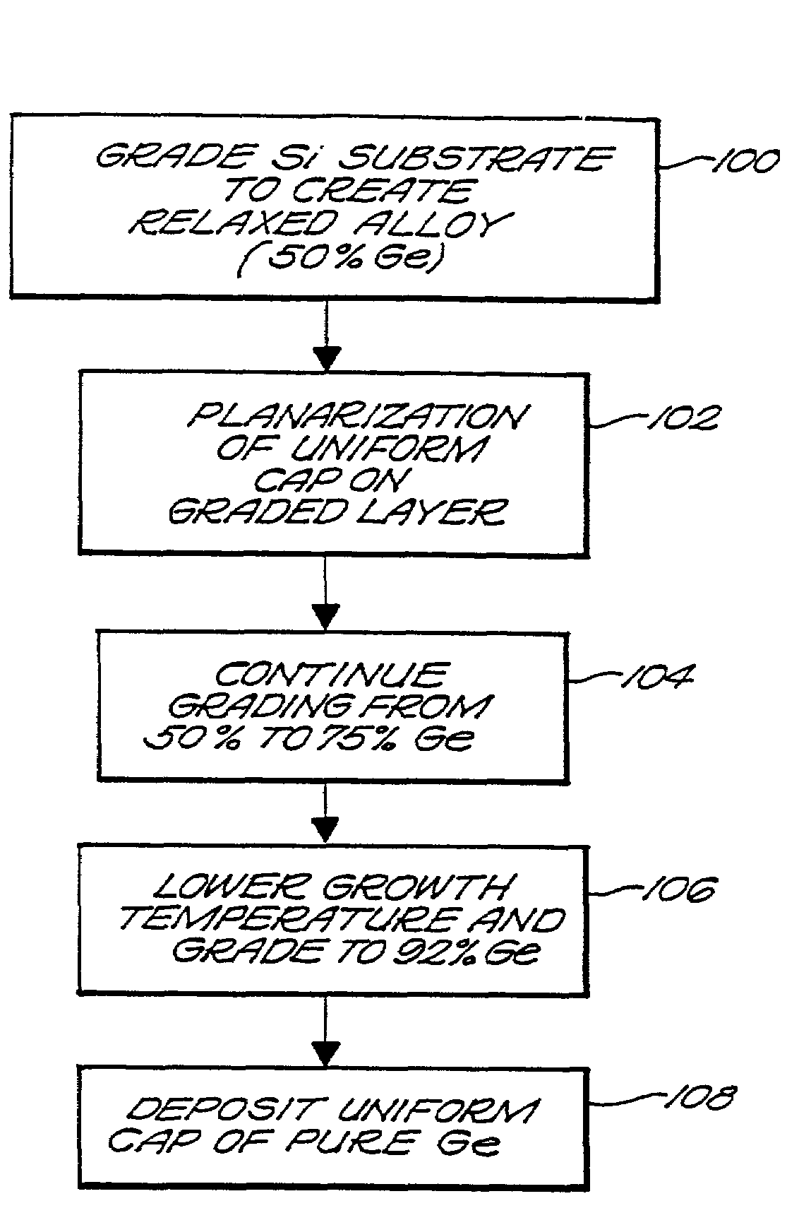
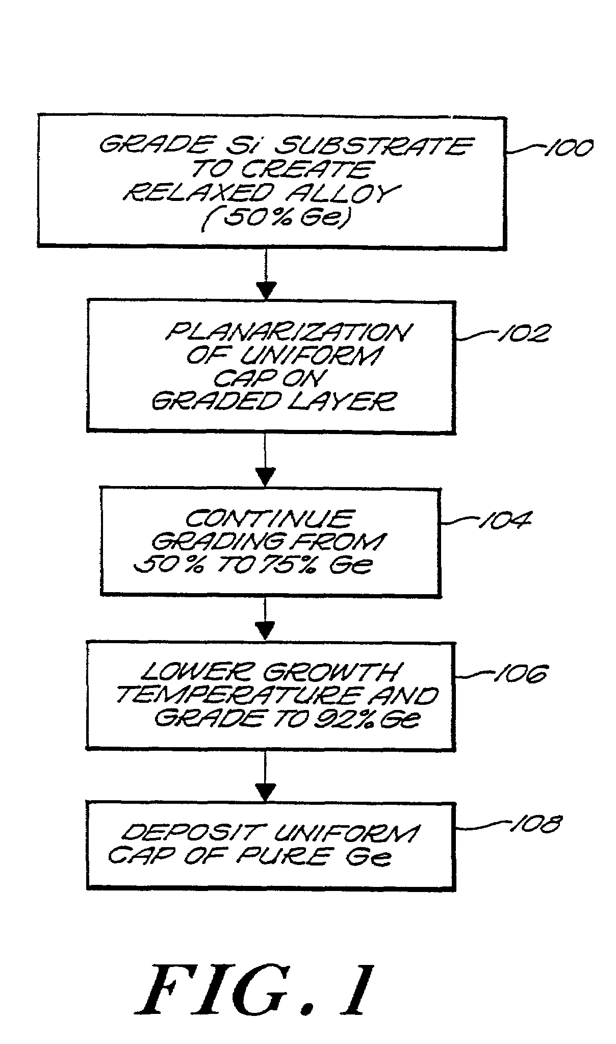
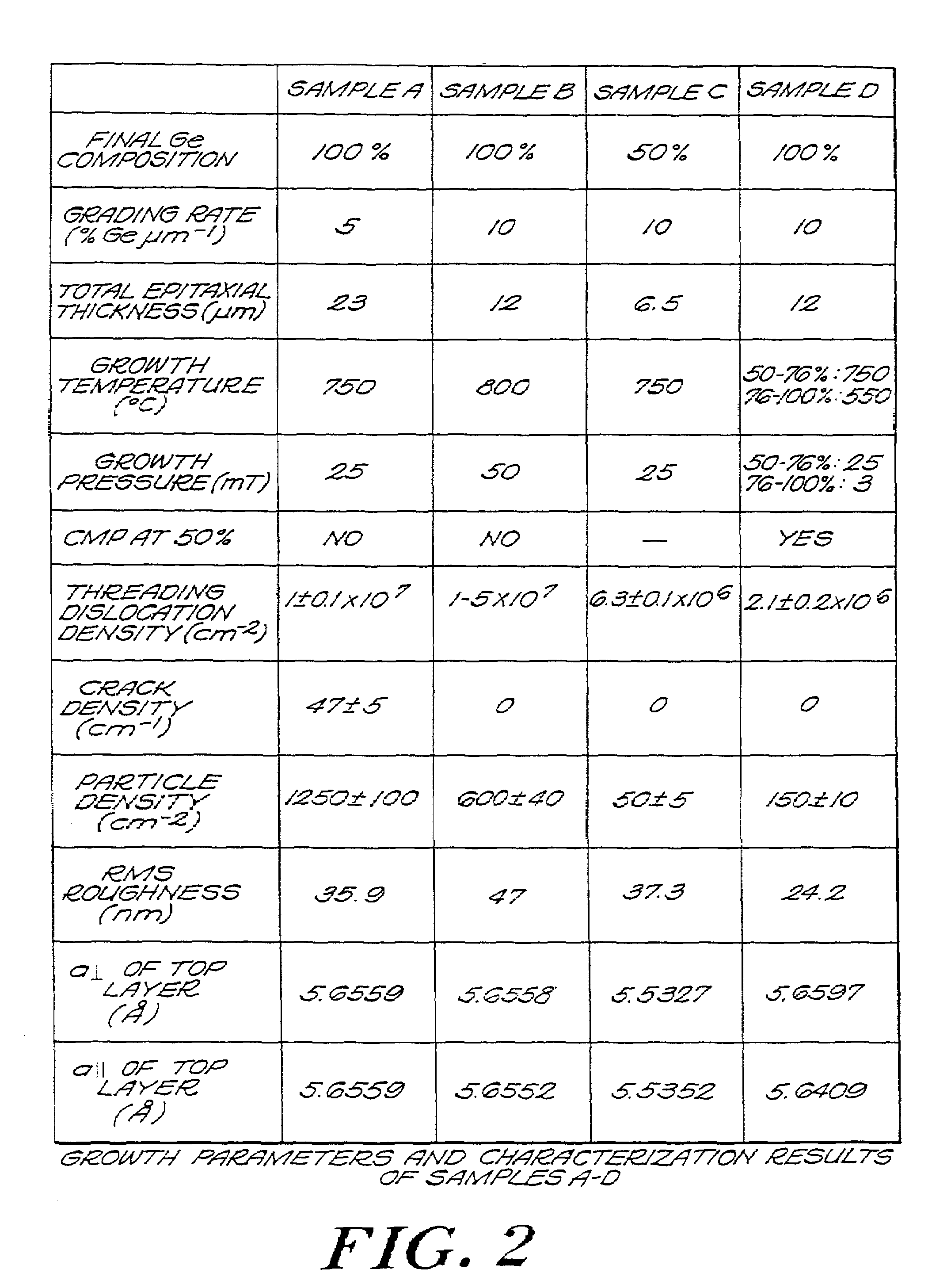
[0018]It has been previously shown that although composition-graded GeSi layers are a viable means to relax GeSi alloys on Si for concentrations 7 cm−2), and the density is certainly greater than relaxed Ge30Si70 on Si using this method (˜7×105 cm−2). The grading rate for such defect densities in Ge30Si70 is 10% Ge per micron of thickness.

[0019]In order to reach the desired goal of lower threading dislocation density, the grading rate is decreased to 5% Ge per micron of thickness. From experience, a lower grading rate will lower the threading dislocation density. However, it was found that the threading dislocation density was nearly equivalent to the 10% Ge / micron grading rate, cracks developed due to the thermal mismatch strain, and many particles were found due to what is believed to be gas-phase nucleation of GeSi since germane cracks at much lower temperatures than silane.

[0020]The major problems that need to be controlled in the semiconductor structure are the cracking and the...


PUM


Abstract

A semiconductor structure including a semiconductor substrate, at least one first crystalline epitaxial layer on the substrate, the first layer having a surface which is planarized, and at least one second crystalline epitaxial layer on the at least one first layer. In another embodiment of the invention there is provided a semiconductor structure including a silicon substrate, and a GeSi graded region grown on the silicon substrate, compressive strain being incorporated in the graded region to offset the tensile strain that is incorporated during thermal processing. In yet another embodiment of the invention there is provided a semiconductor structure including a semiconductor substrate, a first layer having a graded region grown on the substrate, compressive strain being incorporated in the graded region to offset the tensile strain that is incorporated during thermal processing, the first layer having a surface which is planarized, and a second layer provided on the first layer. In still another embodiment of the invention there is provided a method of fabricating a semiconductor structure including providing a semiconductor substrate, providing at least one first crystalline epitaxial layer on the substrate, and planarizing the surface of the first layer.

Description

PRIORITY INFORMATION[0001]This application is a continuation of Ser. No. 09 / 712,604 filed on Nov. 14, 2000 abandoned which is a continuation of Ser. No. 09 / 265,016 filed Mar. 9, 1999, now U.S. Pat. No. 6,291,321 which is a divisional of Ser. No. 09 / 103,672 filed Jun. 23, 1998, now U.S. Pat. No. 6,107,653 which claims priority from provisional applications Ser. No. 60 / 050,602 filed Jun. 24, 1997 and 60 / 059,765 filed Sep. 16, 1997.BACKGROUND OF THE INVENTION[0002]The invention relates to a method of creating flat, crack-free low-dislocation-density mismatched semiconductor layers, and of controlling threading dislocation densities in Ge on Si using graded SiGe layers.[0003]The progression of electronic and optoelectronic components and systems is creating a need for more complex system-level functions to be incorporated at the chip level. One of the effects of this demand is to bring ever-increasing pressure to use materials that are not lattice-matched to common substrates.[0004]The ...

Claims


Application Information

Patent Timeline
Patent Type & Authority Patents(United States)
IPC IPC(8): H01L21/20
CPCH01L21/02381H01L21/02433H01L21/0245H01L21/02502H01L21/02505H01L21/0251H01L21/02532Y10S438/933H01L21/20
Inventor FITZGERALD, EUGENE A.
Owner MASSACHUSETTS INST OF TECH
Learn More