Refresh control method of a semiconductor memory device and semiconductor memory device
a semiconductor memory and control method technology, applied in the field of refresh control, can solve the problems of not being able to achieve sufficient current reducing effect as a whole, the limit of current consumption reduction of the dram, and the inability to reduce the current consumption of the semiconductor memory device at the time of self-refresh, so as to achieve the effect of reducing the size of the holding area itself, and increasing the accumulated charg
- Summary
- Abstract
- Description
- Claims
- Application Information
AI Technical Summary
Benefits of technology
Problems solved by technology
Method used
Image
Examples
first embodiment
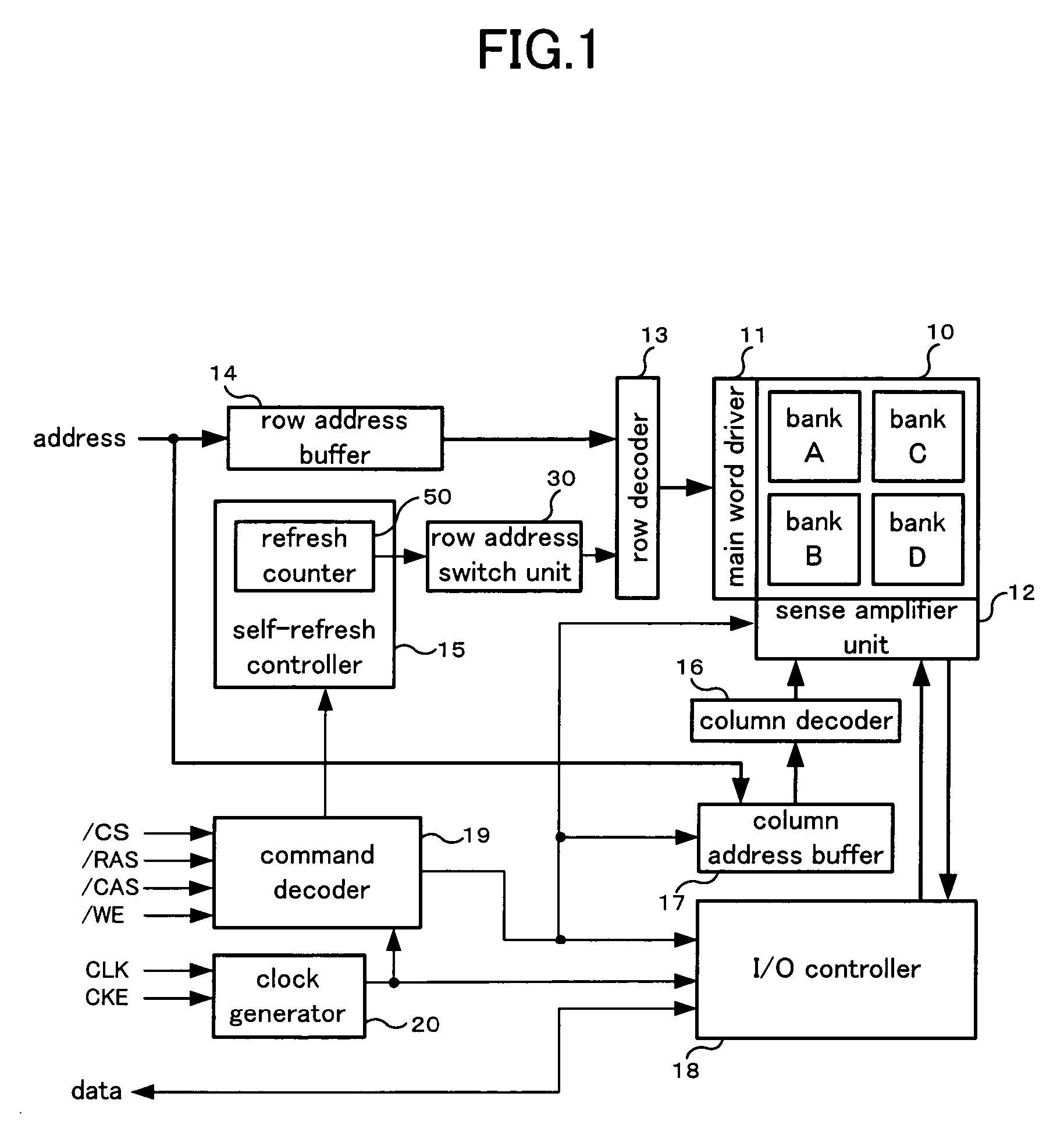
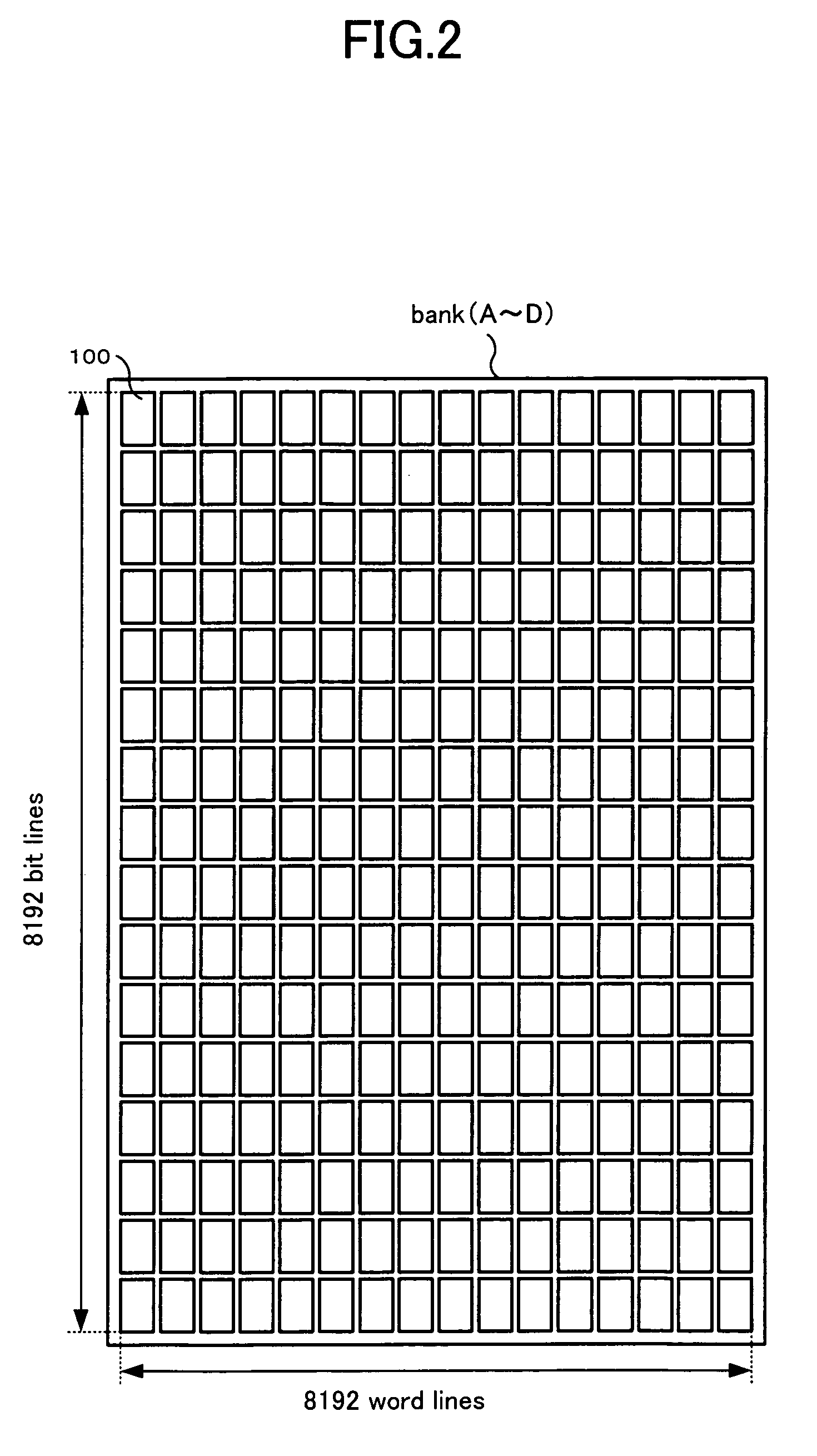
[0076]FIG. 1 is a block diagram showing the entire configuration of a DRAM of a first embodiment. In this example, the DRAM has storage capacity of 256 Mbits, and four banks. The DRAM shown in FIG. 1 has a memory array 10 in which a large number of memory cells are arranged in a matrix form in a direction of rows and in a direction of columns. Each memory cell stores 1 bit. The memory array 10 is divided into four banks which are 64 Mbits storage regions (these banks are shown as banks A, B, C and D in the drawing). These banks have the same configuration. Each bank is designated based on a bank selection signal of 2 bits coming with an address signal.
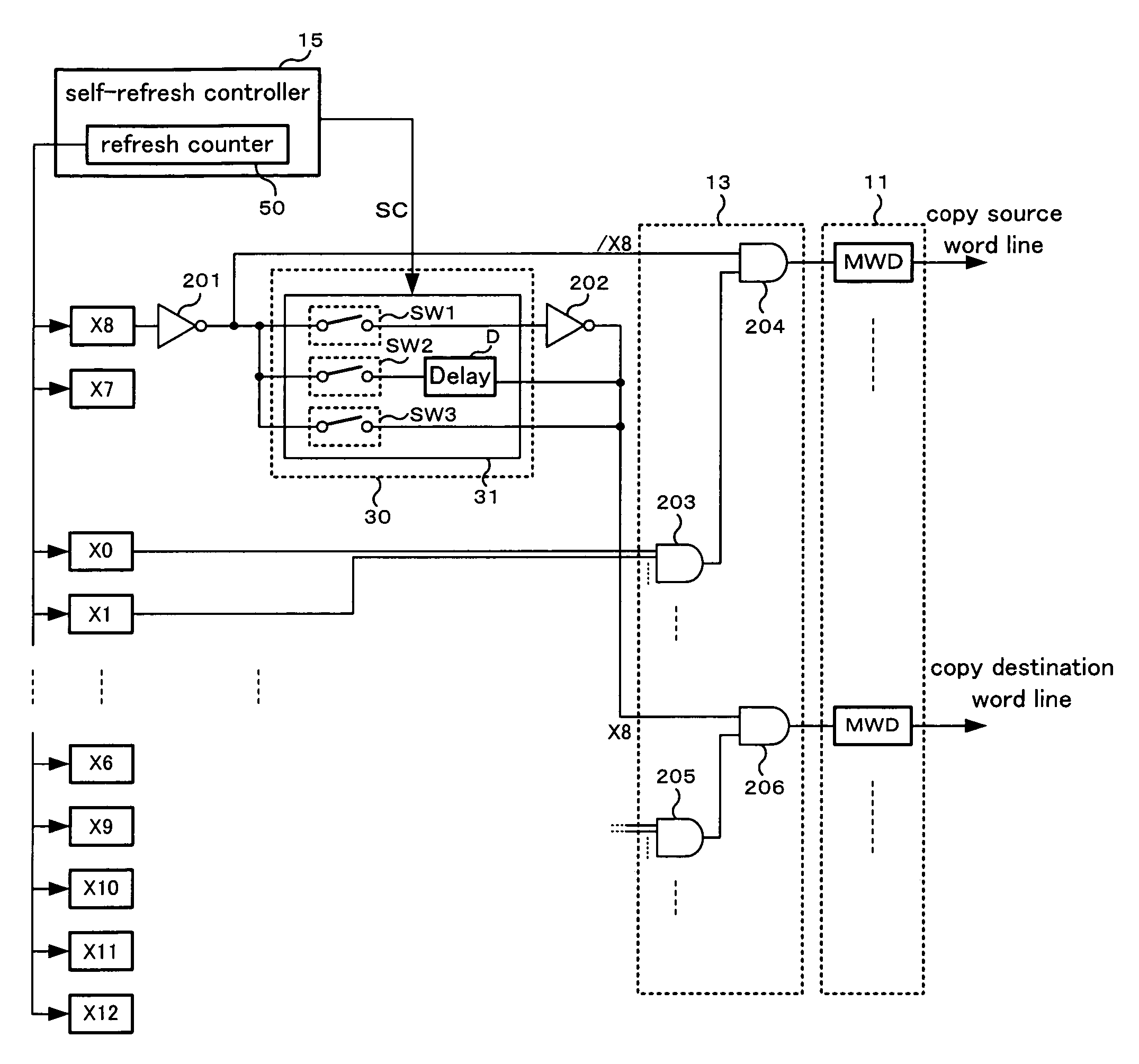
[0077]Provided around the memory array 10 are a main word driver 11, a sense amplifier unit 12, a row decoder 13, a row address buffer 14, a self-refresh controller 15, a column decoder 16, a column address buffer 17, an I / O controller 18, a command decoder 19 and a clock generator 20. Further, a row address switch unit 30 for realizin...
second embodiment
[0156]Next, FIG. 22 is a block diagram showing the entire configuration of a DRAM of a second embodiment which controls the switching operation of the supply voltage in the self-refresh. The entire circuit of the DRAM of the second embodiment is roughly divided into two portions, i.e., an array circuit C1 and a peripheral circuit C2. Basic configurations of the array circuit C1 and the peripheral circuit C2 are common to the DRAM of the first embodiment. In FIG. 22, constituent elements which are common to FIG. 1 are designated with the same numbers.
[0157]In the DRAM of the second embodiment, in addition to the above facts, a power supply unit 60 which generates a supply voltage required for operations of the array circuit C1 and the peripheral circuit C2 and supplies the same to various portions is provided. The power supply unit 60 includes an array power supply 61 which generates supply voltages (array voltages) to be supplied to the array circuit C1, and a peripheral power suppl...
PUM
 Abstract
Description
Claims
Application Information
 - R&D
- Intellectual Property
- Life Sciences
- Materials
- Tech Scout
- Unparalleled Data Quality
- Higher Quality Content
- 60% Fewer Hallucinations
Browse by: Latest US Patents, China's latest patents, Technical Efficacy Thesaurus, Application Domain, Technology Topic, Popular Technical Reports.
© 2025 PatSnap. All rights reserved.Legal|Privacy policy|Modern Slavery Act Transparency Statement|Sitemap|About US| Contact US: help@patsnap.com


