
Integrated color pixel (ICP)

a color pixel and integrated technology, applied in the field of color image sensors, can solve the problems of limited on-chip signal processing capability, high power consumption, and sensitivity variations of sensors, and achieve the effect of reducing the overall height of the pixel

Active Publication Date: 2007-07-24
THE BOARD OF TRUSTEES OF THE LELAND STANFORD JUNIOR UNIV
View PDF22 Cites 70 Cited by
  • Summary
  • Abstract
  • Description
  • Claims
  • Application Information

AI Technical Summary

Benefits of technology

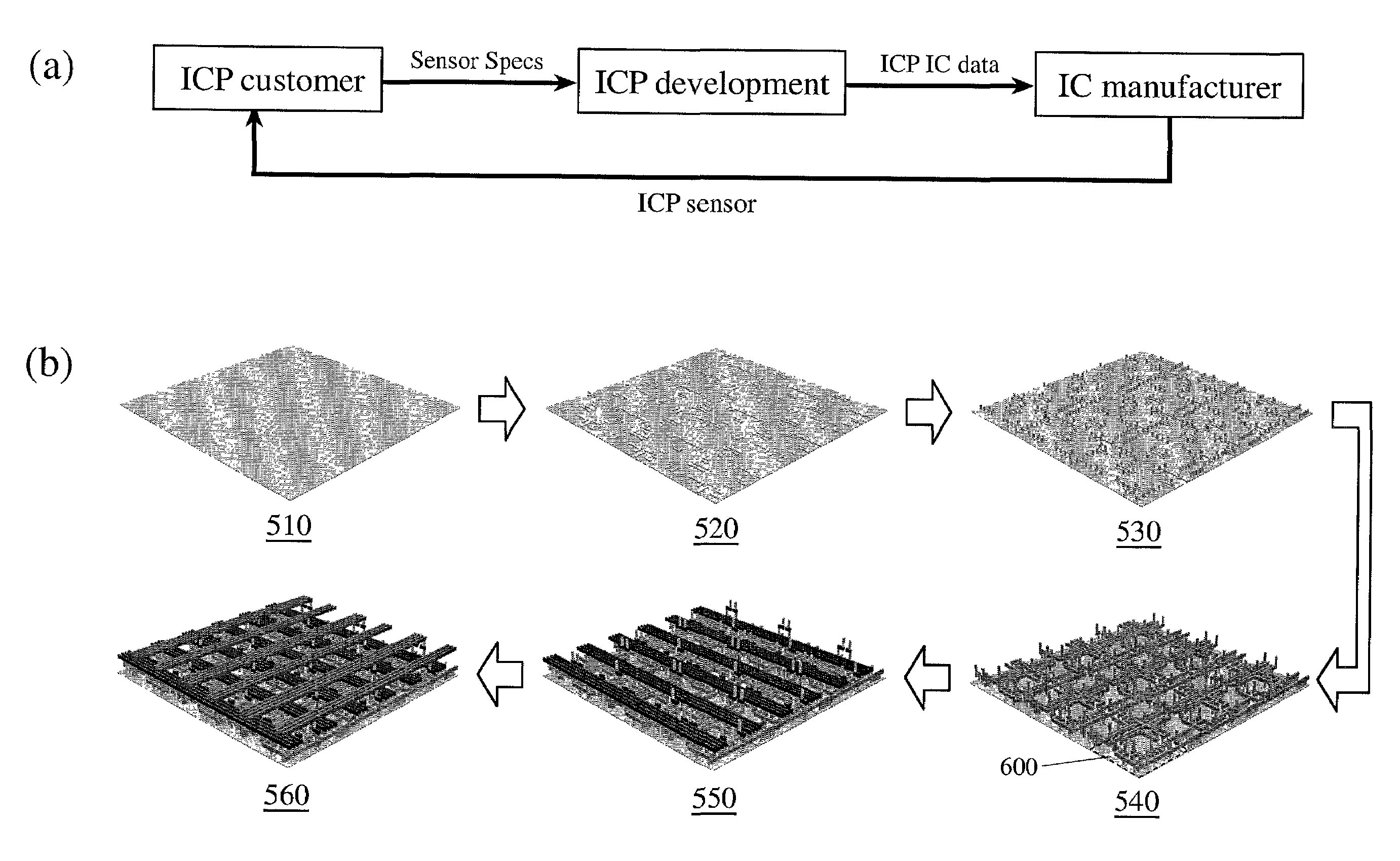
[0022]It is also an object of the present invention to utilize patterned metal layers and / or wires as wavelength selective (color) filter inside the pixel, thereby eliminating a need for additional color filter processing steps or thin films and hence reducing the overall height of the pixel.
[0023]It is yet another object of the present invention to provide an integrated color pixel that provides wavelength selection of light without color cross-talk.

Problems solved by technology

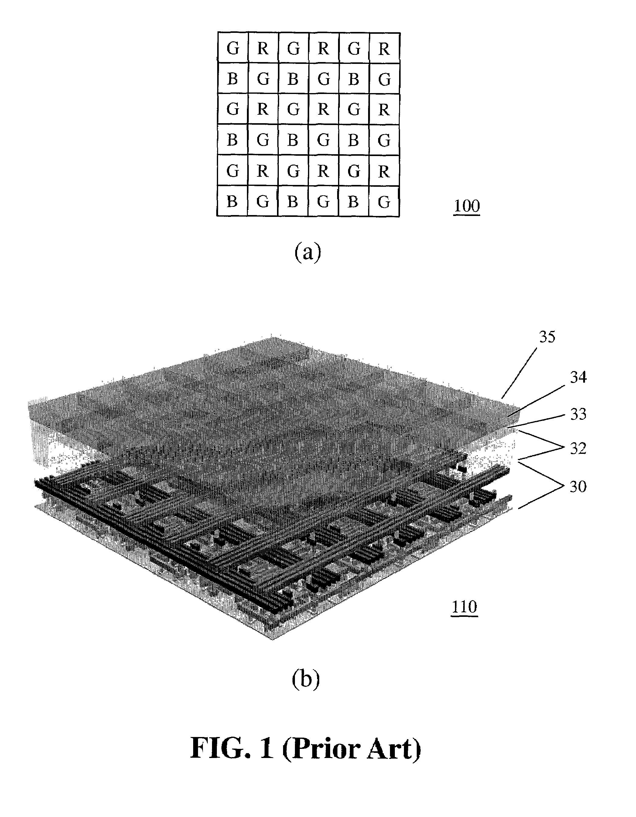
As is well known in the art, one common problem associated with the use of CFA is that pixel and therefore the sensor sensitivity varies with the specific type of color.
CCD image sensors have drawbacks well known in the art including limited on-chip signal processing capability and high power consumption.
CMOS image sensors utilizing CFAs, however, still have the following weaknesses.
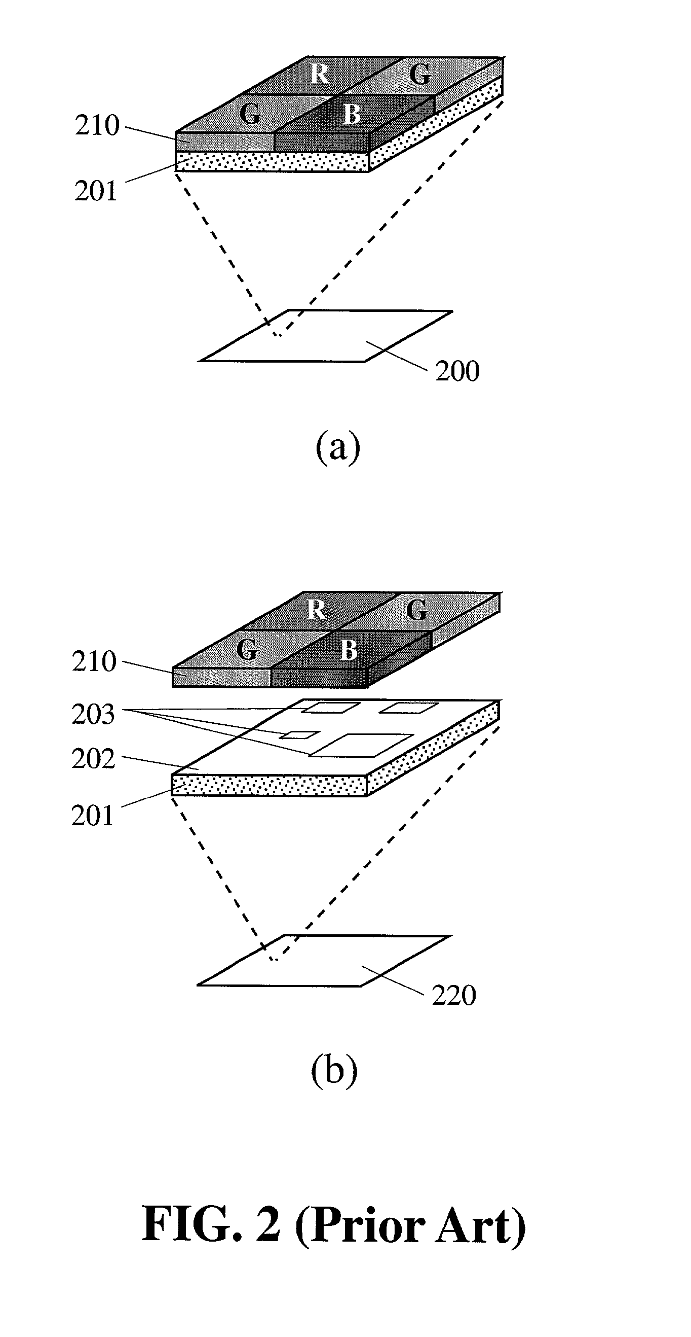
A typical CFA may include multiple layers of superimposed color filters, which often cause a color “cross-talk” problem.
Also, because the height of a pixel inversely affects the pixel's efficiency, the added height of these layers may cause a decrease in pixel efficiency.
The hybrid nature of CMOS image sensors and the color filter process lead to high fabrication costs and inflexibility in color image sensor design flow.
On the other hand, x-Si has poor photoelectric properties but a wide range of highly developed and abundantly available technologies for fabricating powerful integrated circuits.
What is more, pixels in the vertically integrated TFA image sensor having multiple layers deposited thereon may suffer from reduced pixel efficiency because of the increased overall height of the pixels.

Method used


Image

  • Integrated color pixel (ICP)
  • Integrated color pixel (ICP)
  • Integrated color pixel (ICP)

Examples


Embodiment Construction

[0042]The present invention provides a method to control pixel wavelength responsivity during the standard integrated circuit (IC) design and manufacturing process. Rather than utilizing a separate color filter (dye-based, diffraction-based, thin film-based, etc.) the wavelength responsivity is controlled using materials that are integrated into the sensor design itself. That is, the inventive method solely utilizes the semiconductor process for making an ICP image sensor. An ICP of the present invention is thus distinguished from the aforementioned conventional color pixels that are constructed in at least two stages, combining a basic monochrome image sensor with a color filter array or other optical material.

[0043]As is well known in the art, a typical image sensor pixel comprises a light sensitive element (photodetector) that converts photons to electrons and internal circuitry that provides the pixel with desired functionality such as read-out, signal conditioning, and so forth...


PUM


Abstract

An integrated color pixel (ICP) with at least one integrated metal filter is presented. Rather than utilizing a separate color filter, the wavelength responsivity of the ICP is specified and integrated at pixel level into the ICP itself using metal materials already available for standard integrated circuit design and fabrication process. The ICP of the present invention is thus distinguished from a conventional color pixel constructed in a two-stage process that combines an image sensor with a color filter array or other optical material.

Description

BACKGROUND OF THE INVENTION[0001]1. Field of the Invention[0002]The present invention relates generally to a color image sensor and, more particularly, to an integrated color pixel (ICP) and a method of integrating control of wavelength responsivity into the ICP itself during a standard integrated circuit (IC) design and fabrication process.[0003]2. Description of the Related Art[0004]A basic image sensor captures an image in gray scale. That is, the image sensor, with its monochrome pixels, generally records the image in a series of tones ranging from pure white to pure black. A color image sensor captures the image in colors with monochrome pixels and color filters. The color filters are utilized for controlling the wavelength responsivity of the individual monochrome pixels. The wavelength transmittance of the color filters, along with the other optical elements, determine the wavelength responsivity of the color channels of the color image sensor.[0005]A conventional way to inte...

Claims


Application Information

Patent Timeline
IPC IPC(8): H04N5/335H01L31/062H01L27/146H01L31/0216H01L31/0224H04N9/04
CPCH01L27/14621H01L27/14685H01L27/14689H01L31/02165H04N9/045H01L27/14636H01L31/022408H01L27/14868
Inventor CATRYSSE, PETER B.WANDELL, BRIAN A.
Owner THE BOARD OF TRUSTEES OF THE LELAND STANFORD JUNIOR UNIV
Learn More