
Layout method and computer program product

a computer program and layout method technology, applied in the field of layout methods, can solve the problems of increasing the time required for layout operations, affecting the efficiency of layout operations, and easy generation of circuit malfunctions, etc., and achieve the effect of easy creation

Inactive Publication Date: 2007-07-17
SOCIONEXT INC
View PDF5 Cites 13 Cited by
  • Summary
  • Abstract
  • Description
  • Claims
  • Application Information

AI Technical Summary

Benefits of technology

The present invention provides a layout method for an integrated circuit that can securely place required decoupling capacitance in an optimal position, reduce re-execution of placement due to shortage of decoupling capacitance, and easily create virtual cells. The method involves calculating the required decoupling capacitance for every functional cell in advance, creating a virtual cell with the required placement area, and placing the virtual cell on the chip. This reduces the amount of data needed for the virtual cell and allows for easy placement, reducing the time required for the layout design and improving the efficiency of the integrated circuit design process.

Problems solved by technology

In the semiconductor integrated circuit, however, noises are increased according to an increase in speed of operation frequency, and resistance against the noises is deteriorated by lowering voltage, thus causing a problem that circuit malfunction is easily generated by the noises.
For this reason, since the decoupling capacitance is not necessarily placed near a functional cell which particularly requires the decoupling capacitance, for example a functional cell which becomes a source of power supply noise, such as a flip-flop, a clock buffer, or the like, there is a fear that the decoupling capacitance may not effectively function.
For this reason, when there is a shortage of a free area for placing a decoupling capacitance, it is necessary to correct the result of layout processing in order to secure the free area, so that there is a problem of an increase in time required for layout operations.

Method used


Image

  • Layout method and computer program product
  • Layout method and computer program product
  • Layout method and computer program product

Examples


embodiment 1

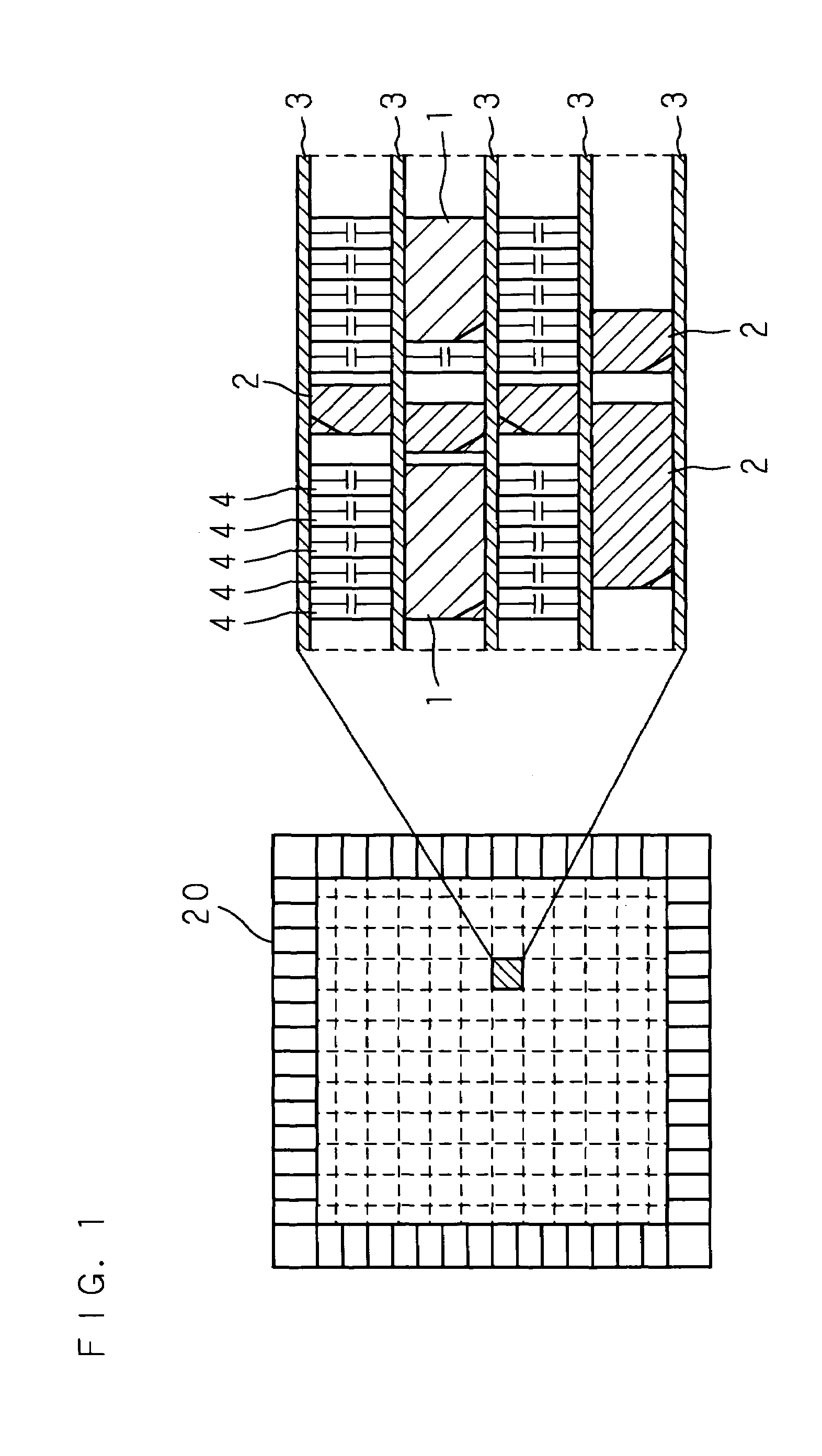
[0050]FIG. 1 is a schematic plan view illustrating a layout of a semiconductor integrated circuit to which the present invention is directed. Here, FIG. 1 also illustrates a schematic plan view of an enlarged portion where a plurality of logic cells are laid out.

[0051]In FIG. 1, reference numeral 20 represents a semiconductor integrated circuit. In the semiconductor integrated circuit 20, there are placed a number of logic cells 1 having high possibility to be a source of noises and a number of logic cells 2 having low possibility to be the source of noises on a semiconductor chip. It should be noted that the logic cell 1 having high possibility to be the source of noises includes, for example, a flip-flop, a clock buffer, and the like, which always operates in conjunction with a clock. The logic cell 2 having low possibility to be the source of noises is the cell, such as a NAND element, a NOR element, and the like, which are placed between the flip-flops to execute a logical opera...

embodiment 2

[0086]In Embodiment 1 described above, the cell library 57 including the virtual cell 10 is created in advance, and then the shrink of the virtual cell 10 is performed at the layout processing. In Embodiment 2, however, the cell library 57 is not created in advance, but the virtual cell 10 is created by adding the decoupling capacitance placement area 5 to the logic cell 1 at the layout processing.

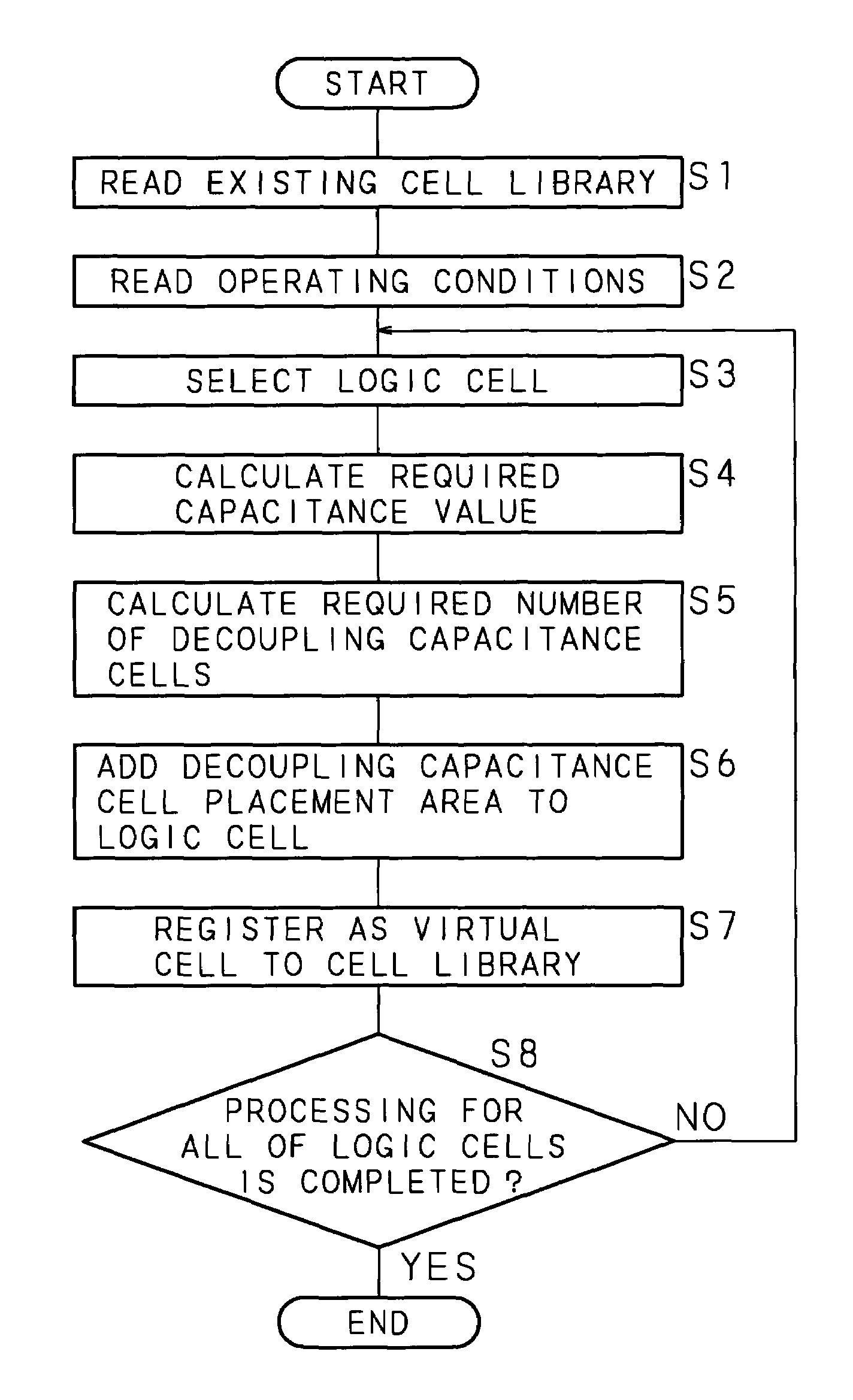
[0087]FIG. 10 is a flowchart illustrating the procedure of the layout processing according to Embodiment 2 of the present invention. It is needless to say that the processing is performed by the CPU 50 according to the program 55.

[0088]The layout processing of Embodiment 2 is started by reading the cell library from the storage device 54 (step S41). The cell library read at this time is not the cell library 57 including the virtual cell 10, but the existing cell library to which the planar shapes of only the logic cells 1 and 2 are registered. Next, from the storage device 54, the circuit ...


PUM


Abstract

A required value of decoupling capacitance is calculated in advance for every functional cell, a virtual cell which has a functional cell, and a decoupling capacitance placing area required for placing the decoupling capacitance with the calculated value is created, the virtual cell is placed on a chip, and the decoupling capacitance cell is subsequently placed in the decoupling capacitance placing area of the virtual cell. A layout method of an integrated circuit and a computer program, in which a decoupling capacitance with an amount required for preventing malfunction caused by a noise can be surely placed, and there is no possibility that the functional cell will need to be replaced due to a shortage of the decoupling capacitance after placing the functional cell can be realized.

Description

CROSS-REFERENCE TO RELATED APPLICATIONS[0001]This Nonprovisional application claims priority under 35 U.S.C. §119(a) on patent application No. 2005-336279 filed in Japan on Nov. 21, 2005, the entire contents of which are hereby incorporated by reference.BACKGROUND OF THE INVENTION[0002]1. Field of the Invention[0003]The present invention relates to a layout method of a semiconductor integrated circuit provided with a decoupling capacitance for preventing malfunction caused by noises of power supply, also relates to a computer program product for causing a computer to execute such a layout method.[0004]2. Description of Related Art[0005]In recent years, microfabrication and high integration of a semiconductor integrated circuit have been achieved, and in connection with this, a lowering in operating voltage, an increase in speed of operating frequency, and the like have been made. For example, a process rule of manufacturing the semiconductor integrated circuit has been reduced to 0....

Claims


Application Information

Patent Timeline
Patent Type & Authority Patents(United States)
IPC IPC(8): G11C5/02
CPCG06F17/5072G06F30/392
Inventor INOUE, YOSHIO
Owner SOCIONEXT INC
Learn More