Eureka AIR delivers breakthrough ideas for toughest innovation challenges, trusted by R&D personnel around the world.

Electron beam apparatus and device fabrication method using the electron beam apparatus

a technology of electron beam and electron beam, which is applied in the field of electron beam apparatus and device fabrication method using electron beam apparatus, can solve the problems of reducing the quality of sem images, requiring a huge amount of time for inspection, etc., and achieve the effect of improving throughpu

Inactive Publication Date: 2007-07-17
EBARA CORP
View PDF34 Cites 66 Cited by
  • Summary
  • Abstract
  • Description
  • Claims
  • Application Information

AI Technical Summary

Benefits of technology

[0005]It is therefore the basic objective of the present invention to make improvements to prior multibeam scanning systems, and more specifically, to provide better throughput.
[0007]Also, to improve the accuracy of inspections of samples performed using electron beams, the present invention provides an electron beam inspection apparatus configured to provide more precise axial alignment of its electron optical systems. More specifically, alignment of the axes of the multiple beams is performed by adjusting the elements of the optical system such that when voltages applied to the elements (lenses, etc.) of the electron optical system are changed, electron beams that are the same distance from the center of the multiple beams will exhibit substantially the same amount of change in position on the sample.
[0010]In addition, provided in another aspect of the multibeam inspection apparatus of the present invention, is an electron beam inspection apparatus in which is provided a correction device for irradiating irradiation design points with primary electron beams, to thereby establish good optical conditions for performing inspections.
[0012]The present invention also provides an electron beam inspection apparatus in which shot noise is reduced, by establishing conditions such that the electron gun is operated in the space-charge-limited region of its characteristic curve.
[0014]In addition, the present invention provides an electron beam inspection apparatus wherein the electron optical elements such as electron lenses and deflectors that make up its optical systems are constructed such that, rather than using fasteners such as bolts to join the separate insulators and conductors provided therein, conductive layers are formed on required areas of the insulators by electroplating, to thus provide compact electron optical elements of simple construction.

Problems solved by technology

Because of the small beam size, pixel size, and raster width used in SEM systems adapted for defect inspection, however, such inspections required a huge amount of time.
Also, when the sample was irradiated with a larger beam to improve throughput, this produced degraded spacial resolution quality of the SEM images.

Method used


Image

  • Electron beam apparatus and device fabrication method using the electron beam apparatus
  • Electron beam apparatus and device fabrication method using the electron beam apparatus
  • Electron beam apparatus and device fabrication method using the electron beam apparatus

Examples


third embodiment

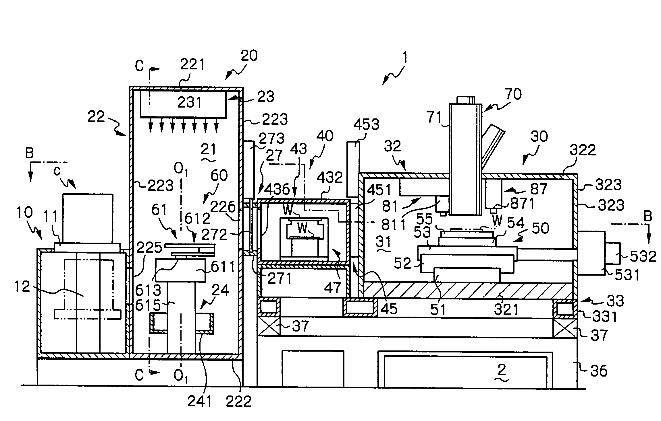
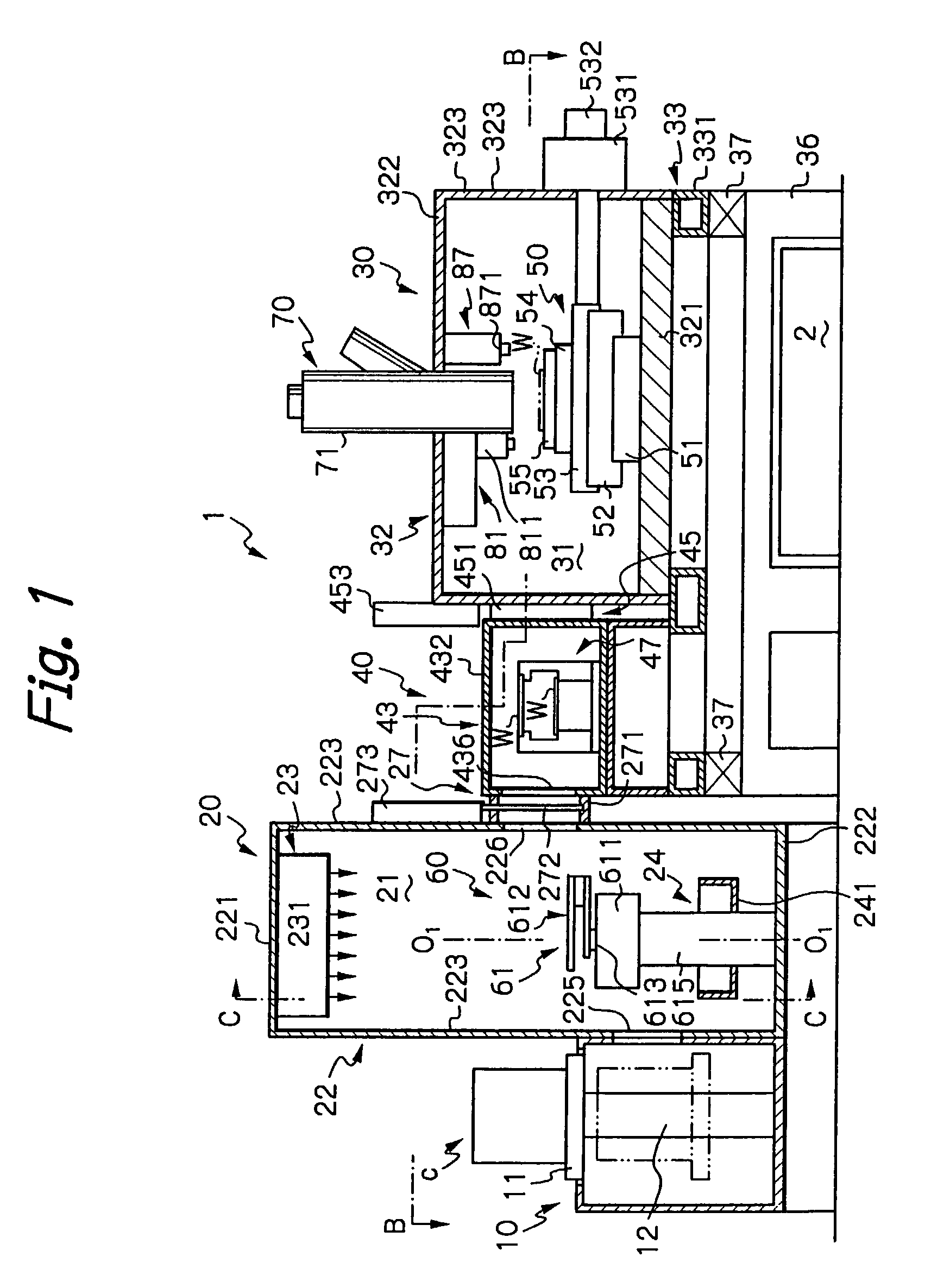
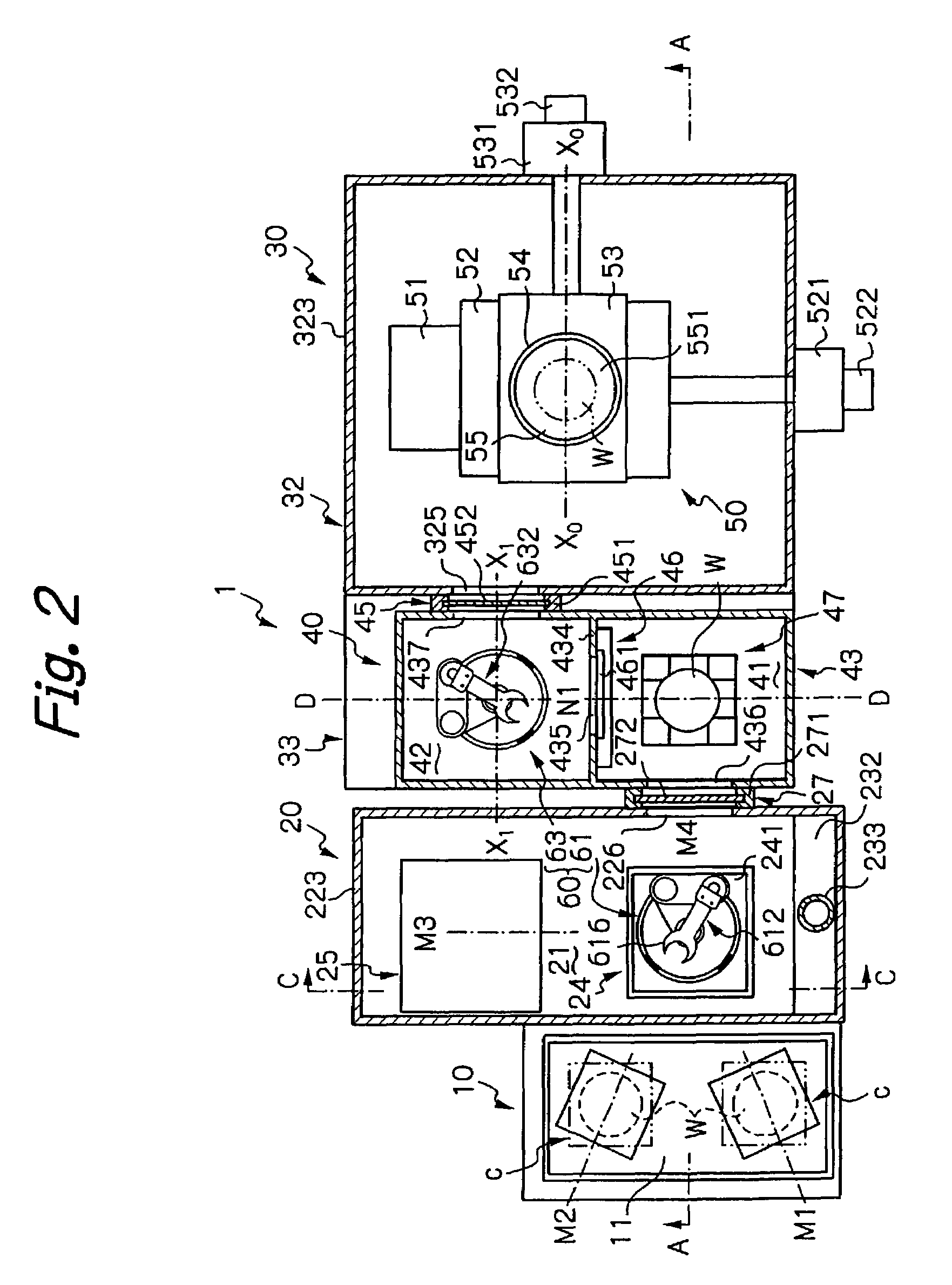
[0252]A third embodiment, shown in FIG. 24 uses essentially the same configuration as that described above (Stage Improvement 1, for improving the maintenance of stable vacuum in the working chamber). In this embodiment, a diaphragm 19-3 with a built-in differential discharge structure is provided around the electron beam irradiator 2-3 of the column 1-3. The diaphragm 19-3 is cylindrical in shape, and has a circular channel 20-3 formed inside, with a pumping path 21-3 extending upward from the circular channel. This discharge path connects to a vacuum line 23-3 through an internal space 22-3. An ultra-fine gap of from a few tens of μm to a few mm is formed between the bottom end of the diaphragm 19-3 and the top surface of the sample S.

[0253]In this configuration, when gas is emitted from the stage during its movement, raising the pressure in the chamber C, and thus urging a flow of gas into the electron beam irradiator 2-3 (output end of the column), because the diaphragm 19-3 has...

fourth embodiment

[0255]A fourth embodiment is shown in FIG. 25. A diaphragm 26-3 is provided around a chamber C and an electron beam irradiator 2-3, for separating the electron beam irradiator 2-3 from the chamber C. This diaphragm 26-3 is connected through a support member 29-3 (made of a material that is a good conductor, such as copper or aluminum) to a refrigeration unit 30-3, which cools it to between −100° C. and −200° C. A member 27-3, for blocking thermal conduction between the chilled diaphragm 26-3 and the column, is made of a material of poor thermal conductivity, such as a ceramic or resin. Also, a member 28-3, made of a non-insulating ceramic, etc., is formed at the bottom end of the diaphragm 26-3, to prevent discharge between a sample S and the diaphragm 26-3.

[0256]Through such a configuration, gas molecules attempting to flow from the chamber C to the electron beam irradiator are blocked by the diaphragm 26-3, and any gas that does manage to enter is frozen onto the surface of the di...

fifth embodiment

[0258]A fifth embodiment is shown in FIG. 26. Provided on the two movable units of the stage 3-3 are the same diaphragms 12-3 and 14-3 as are shown in FIG. 22. Therefore, regardless of where the sample stage 4-3 is moved, these diaphragms, through the gap closure stops 50-3 and 51-3, wall partition off the inner space 13-3 from the chamber C. In addition, formed around the electron beam irradiator 2-3 is a diaphragm 16-3 like the one shown in FIG. 23, for partitioning off the inside of the chamber C from the electron beam irradiator 2-3 space 24-3, through a gap closure stop 52-3. Through this configuration, when gas adsorbed during stage movement is discharged into the space 13-3, raising the pressure in this portion, any increase in pressure in the chamber C can be suppressed, and any pressure increase within the space 24-3 can be even further suppressed. In this manner, the pressure in the electron beam irradiation space 24-3 can be maintained in a low pressure state. Also, a dif...


PUM


Abstract

The purpose of the invention is to provide an improved electron beam apparatus with improvements in throughput, accuracy, etc. One of the characterizing features of the electron beam apparatus of the present invention is that it has a plurality of optical systems, each of which comprises a primary electron optical system for scanning and irradiating a sample with a plurality of primary electron beams; a detector device for detecting a plurality of secondary beams emitted by irradiating the sample with the primary electron beams; and a secondary electron optical system for guiding the secondary electron beams from the sample to the detector device; all configured so that the plurality of optical systems scan different regions of the sample with their primary electron beams, and detect the respective secondary electron beams emitted from each of the respective regions. This is what makes higher throughput possible. To provide high accuracy, the apparatus is configured such that the axes of its optical systems can be aligned, and aberrations corrected, by a variety of methods.

Description

BACKGROUND OF THE INVENTION[0001]The present invention is related to an apparatus for using a plurality of electron beams to inspect for defects, etc., in patterns formed on the surface of a sample; and in particular, to an apparatus for performing high-throughput wafer defect detection (such as, for example, in a semiconductor device fabrication process) by irradiating the sample with an electron beam; detecting secondary electrons (which vary according to the properties of the surface of the sample); forming image data therefrom; and inspecting and evaluating patterns, etc., formed on the surface of the sample, based on that image data. It is also related to a device fabrication method for high yield production of semiconductor devices, using such an apparatus.[0002]Conventional systems using scanning electron microscopes (SEM) are currently available for performing the above wafer inspection function. These systems form an SEM image by raster-scanning a finely focussed electron b...

Claims


Application Information

Patent Timeline
IPC IPC(8): H01J37/28G01N23/22H01J37/256G01N23/225H01J37/06H01J37/073H01J37/18H01J37/20H01J37/22H01J37/244
CPCG01N23/225G01N23/2251H01J37/06H01J37/073H01J37/185H01J37/20H01J37/222H01J37/244H01J37/28H01J2237/082H01J2237/202H01J2237/20228H01J2237/204H01J2237/22H01J2237/24564H01J2237/2806H01J2237/2816H01J2237/2817
Inventor NAKASUJI, MAMORUSATAKE, TOHRUNOJI, NOBUHARUSOBUKAWA, HIROSIKARIMATA, TSUTOMUYOSHIKAWA, SHOJIKIMBA, TOSHIFUMIOOWADA, SHINSAITO, MUTSUMIHAMASHIMA, MUNEKIKOHAMA, YOSHIAKIOKUBO, YUKIHARU
Owner EBARA CORP
Why Eureka
Eureka Blog
Learn More