
Production method for a multilayer ceramic substrate

a production method and ceramic substrate technology, applied in the direction of solid-state devices, electrical devices, metal-patterned materials, etc., can solve the problems of low degree of flexibility in design, difficult to put molded body blocks into the spaces in the laminated body with high accuracy, and occurrence of separation between the substrates. , the effect of increasing the degree of flexibility in circuit design

Inactive Publication Date: 2007-07-17
TDK CORPARATION
View PDF22 Cites 5 Cited by
  • Summary
  • Abstract
  • Description
  • Claims
  • Application Information

AI Technical Summary

Benefits of technology

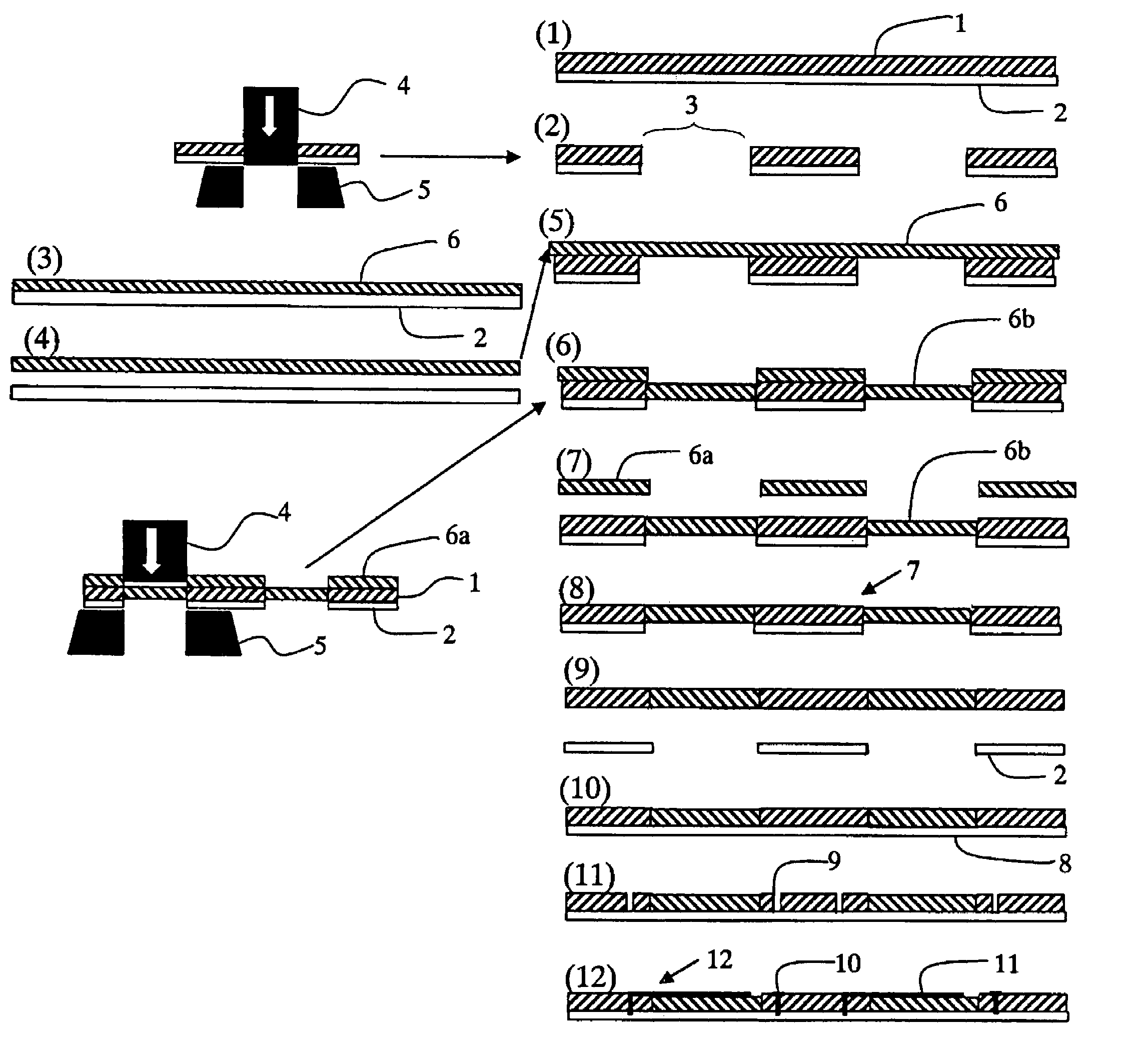
[0011]Therefore, an object of the invention is to provide a multilayer ceramic substrate characterized in that: (1) different dielectrics are electrically connected to each other in the direction of main surface of a sheet, whereby the degree of flexibility in design is increased and the substrate is made compact in size; (2) dielectrics are formed in required sizes in necessary portions as compared with the laminated structure disclosed in patent document 1, whereby limitations of material physical properties (firing shrinkage, coefficient of thermal expansion) of dielectrics to be combined can be relaxed; and (3) different dielectrics are inserted in desired portions with high accuracy. In addition, another object of the invention is to provide a method of manufacturing a multilayer ceramic substrate having the features described above.
[0025]In the invention, the different dielectrics are electrically connected to each other in the direction of main surface of the sheet, so that the degree of flexibility in circuit design can be increased and the substrate itself can be made compact in size. Further, the dielectrics can be formed in necessary sizes only in necessary portions and the dielectrics to be combined can be selected comparatively freely without limitations of firing shrinkage and coefficient of thermal expansion. Still further, because the different dielectrics are inserted in predetermined portions with accuracy, the occurrence of separation and cracks can be also prevented.

Problems solved by technology

However, in the technology disclosed in patent document 1, dielectrics are arranged in layers in the substrate, so that the degree of flexibility in design is low.
Further, in the technologies disclosed in patent documents 2 to 5, the respective parts can be connected to each other only in the direction of thickness of the substrate, so that the degree of flexibility in design is low.
Also, it is difficult to put the molded body blocks into the spaces in the laminated body with high accuracy.
Still further, gaps are apt to be produced between the parts to decrease reliability.
In addition, the laminated body and the molded body blocks are different from each other 90 degrees in the direction of lamination, so that it is difficult to adjust the spatial size of the laminated body and the sizes of the molded body blocks and unnecessary spaces are required for the adjustment.

Method used


Image

  • Production method for a multilayer ceramic substrate
  • Production method for a multilayer ceramic substrate
  • Production method for a multilayer ceramic substrate

Examples


example 1

[0058]A multilayer ceramic substrate having a capacitor element shown in FIG. 3 was formed, and capacitance and IR were measured. A fired layer 21 of the first green sheet was made to have a composition (SiO2—B2O3—Al2O3—MgO—CaO—SrO) whose dielectric constant ε was 7.3 after firing. A fired layer 22 of the second green sheet was made to have a composition (SiO2—Al2O3—La2O3—B2O3—BaO—TiO2—Bi2O3—Nd2O3—SrO) whose dielectric constant e was 21.1 after firing. The size after firing of the second green sheet inserted in the first green sheet was made 2.57 mm×2.57 mm×40 μm. The size of an internal electrode was 2.13 mm×2.13 mm. An external electrode is denoted by a reference numeral 23. This was Example 1.

example 2

[0059]Similarly, the fired layer 21 of the first green sheet was made to have a composition (BaO—Al2O3—SiO2—B2O3) whose dielectric constant ε was 5.9 after firing. The fired layer 22 of the second green sheet was made to have a composition (BaO—Nd2O3—TiO2—B2O3—CaO—ZnO) whose dielectric constant ε was 72.3 after firing. The size after firing of the second green sheet 22 inserted in the first green sheet 21 was made 2.57 mm×2.57 mm×40 μm. The size of the internal electrode was made 1.71 mm×1.71 mm. This was Example 2.

[0060]The relationship between capacitor capacity and insulation resistance of Example 1, which was measured under conditions that a frequency for capacity measurement was 1 kHz and a voltage for IR measurement was 10 V, is shown in FIG. 4. The relationship between capacitor capacity and insulation resistance of Example 2, which was measured under conditions that a frequency for capacity measurement was 1 kHz and a voltage for IR measurement was 10 V, is shown in FIG. 5. ...


PUM

PropertyMeasurementUnit
timeaaaaaaaaaa
heating temperatureaaaaaaaaaa
pressing pressureaaaaaaaaaa

Abstract

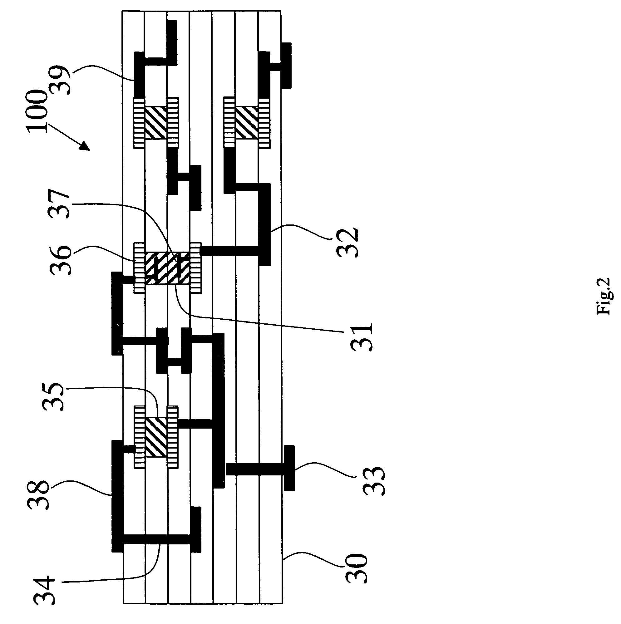
An object of the invention is to connect different dielectrics electrically to each other in the direction of main surface of a sheet in a multilayer ceramic substrate and to increase the degree of flexibility in design and make the multilayer ceramic substrate compact in size. A multilayer ceramic substrate in accordance with the invention is formed of a plurality of laminated ceramic substrates including such a composite ceramic substrate of different materials that is made by inserting the second ceramic substrate in a pounched-out portion made in the first ceramic substrate and by planarizing its top and bottom surfaces, wherein a conductive layer is formed in a portion across a boundary between the first ceramic substrate and the second ceramic substrate of the interface of the composite ceramic substrate of different materials.

Description

CROSS-REFERENCE TO RELATED APPLICATIONS[0001]This application claims priority of the Japanese Patent Application No. 2004-054271 filed on Feb. 27, 2004.BACKGROUND OF THE INVENTION[0002]1. Field of the Invention[0003]The invention relates to a multilayer ceramic substrate constructed of a combination of a plurality of ceramic materials having electric characteristics and / or physical characteristics that are different from each other and a its production method.[0004]2. Description of the Related Art[0005]A multilayer ceramic substrate is formed of a plurality of ceramic layers and conductive lines are formed along the interfaces between the respective ceramic layers. Usually, the multilayer ceramic substrate is manufactured by laminating green sheets of plural kinds of ceramic materials having electric characteristics and / or physical characteristics that are different from each other so as to achieve multiple functions and high performance and by firing the produced composite laminat...

Claims


Application Information

Patent Timeline
Patent Type & Authority Patents(United States)
IPC IPC(8): H01K3/10C04B35/622C04B35/00C04B35/495H01G4/06H01G4/20H05K1/03H05K1/09H05K1/16H05K3/00H05K3/46
CPCH05K1/162H05K1/0306H05K3/005H05K3/4611H05K3/4629H05K2201/0187Y10T156/1057Y10T29/49165Y10T428/24322Y10T156/1056Y10T29/49163Y10T29/49155Y10T29/49162H05K3/46
Inventor HATANAKA, KIYOSHINISHINO, HARUONINOMIYA, HIDEAKI
Owner TDK CORPARATION
Learn More