
Integrated circuit chip design

a technology of integrated circuits and chips, applied in the direction of cad circuit design, program control, instruments, etc., can solve the problems of huge project risk in dependent upon any job, no good way to benefit from parallel work, and loss of hierarchy

Inactive Publication Date: 2007-07-10
MORPHICS TECH +1
View PDF32 Cites 50 Cited by
  • Summary
  • Abstract
  • Description
  • Claims
  • Application Information

AI Technical Summary

Benefits of technology

[0004]Improvement in the flat capacity of CAD tools still doesn't obviate the need for a hierarchical flow for top-end designs. A “truly hierarchical” flow supports making replicated instances of blocks that share a single abstraction each of their logic, timing, routing, and port location models. If different instances must end up having separate models anyway, then much of the advantage of hierarchy is lost. The point is that replicated block instances be used as truly identical objects so that the various design and analysis tasks done at a block level do not have to be repeated for each instance.
[0007]Partitioning of a design serves to break it into manageable pieces that can benefit from the parallelized effort of the individuals in a team. The goal is to allow separable progress of the work both for individual blocks and concurrently at the top-level. Another reason why flat approaches fail to provide timing convergence is because there is no good way to benefit from parallel work if final timing or routing is bottlenecked through single large runs. Instead, partitioning allows multiple people and licenses to be applied effectively. A good goal is to seek “equalized pain” between blocks and their parent in a hierarchical design, so that the block size is small enough that the effort of routing and timing closure at a block level is about the same as the effort required for their parent.
[0012]By de-rating the idealized velocity (for example, by cutting it in half), a design team can choose a velocity that will have enough margin for the realities of non-ideal repeater locations, non-ideal actual wire paths due to routing congestion, and fan-out prior to the next repeater along each branch. A top-level timing analysis can then combine the input arrival times and departure times of each block's ports with a timing of the parent's signals using the de-rated signal velocity on the Manhattan (x+y) distance pairwise between each output port and every input port it drives. In this way, top-level timing budgets and wirelengths can be driven to meet design goals and to prevent wires that have to cross the full chip, since this would take several clock cycles at today's frequencies.Abstraction
[0019]Furthermore, the paths used for these checks need to include the clock trees going back to the point of reconvergence between the parts of the clock distribution tree feeding the launching and receiving register. Thus, ordinary setup and hold checks also validate the quality of the clock distribution tree, emphasizing local skew instead of global skews, and allow for the possibilities of using “useful skew”, as well as not penalizing bad skew where it wouldn't make any difference to the affected set up or hold checks anyway.
[0020]This rigorous and safe approach to clock tree analysis allows a much lower-power clock distribution scheme using tall clock trees with limited average fan-out, rather than the overkill of more common short-fat solutions that sometimes expend a third of the switching capacitance of the chip just in distributing a core clock.

Problems solved by technology

If different instances must end up having separate models anyway, then much of the advantage of hierarchy is lost.
Another reason why flat approaches fail to provide timing convergence is because there is no good way to benefit from parallel work if final timing or routing is bottlenecked through single large runs.
Further, for many reasons, there are huge project risks in depending upon any job that would take multiple days of runtime to complete because it might never complete due to power failures or program bugs that don't become apparent until too late.
Even though tools could support blocks several times this size, it is less optimal for the overall project because individual blocks with 1M gates just take too long in runtime for all steps, and are too close to failing completely due to lack of real or virtual memory, even on machines with many gigabytes of memory.
One of the classic traps that some design approaches fall into, even after doing the hard work of partitioning and floorplanning, is to then choose analysis methods that don't preserve the isolation between parent and child in the hierarchy.
While modeling solid-sheets of metal would be even more conservative, it is overkill, since the reality in the routed environment will be, at worst, the full-density grids of wires at the routing pitch.
Another classic trap that makes hierarchy less effective is the handling of the timing of the signals crossing the hierarchical boundaries.
The quality of separation is lost if the child timing depends on how much load is applied to a signal by a parent, or if the parent timing depends upon how much internal routing is put on a wire before it gets to an output port.
The effect of simultaneous switching cannot be ignored, but it is also unrealistic to seek a precise determination of when every coupling combination can occur over the range of process spread.
Sometimes, because of the conservative handling of minimum and maximum delay calculations, it can be a tricky balancing act to add delay elements in just the right way to fix the hold violations without degrading the setup paths too much.

Method used


Image

  • Integrated circuit chip design
  • Integrated circuit chip design
  • Integrated circuit chip design

Examples


Embodiment Construction

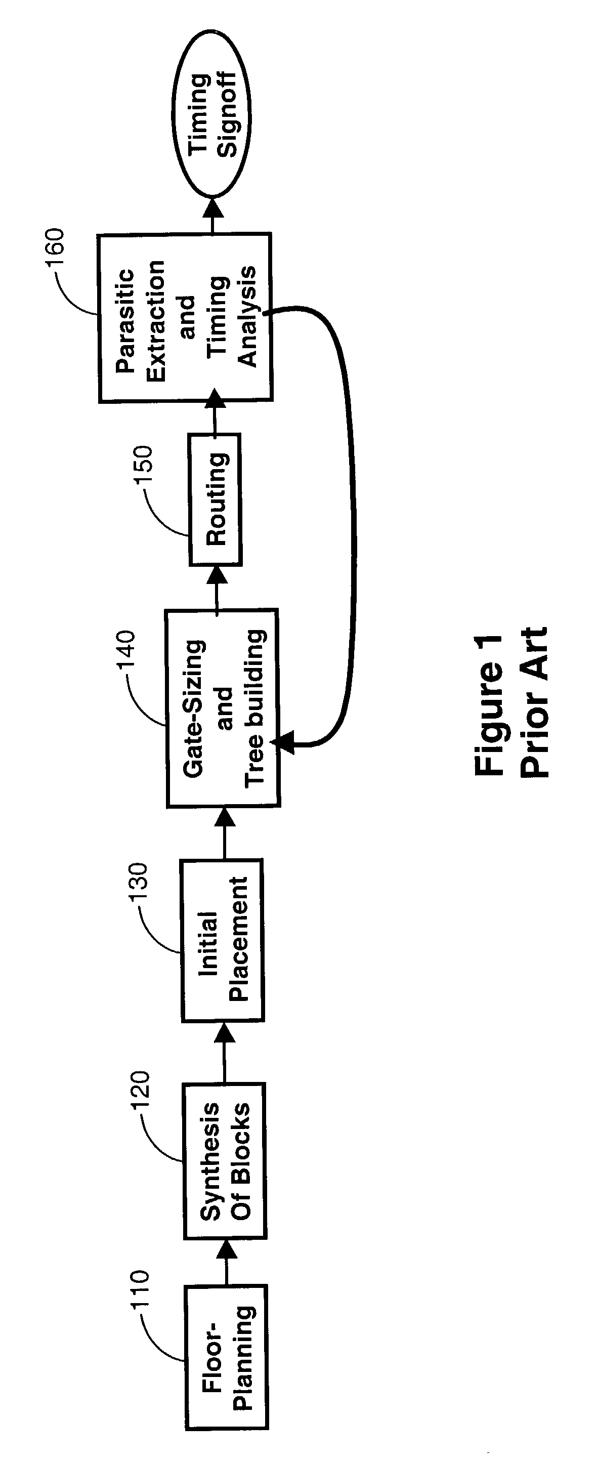
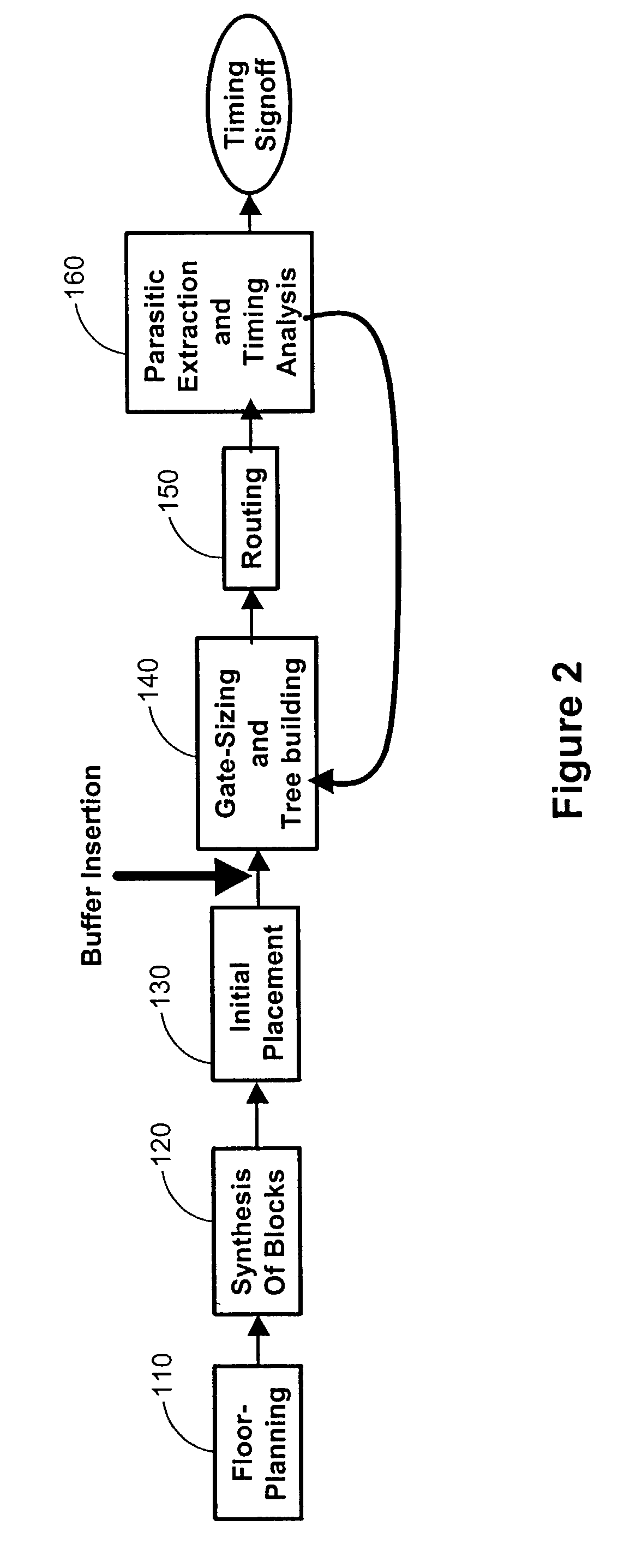
[0039]FIG. 1 depicts the steps conventionally followed in layout of an IC. These steps include floorplanning 110, block synthesis 120, initial placement of blocks 130, gate sizing and clock tree building 140, routing 150, and parasitic extraction and timing analysis 160.

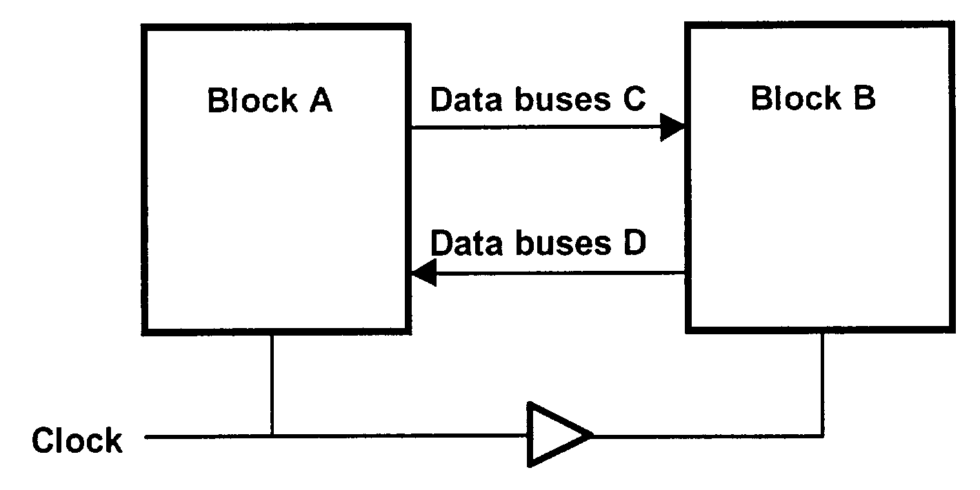
[0040]Timing analysis is ordinarily performed at the end of the process because of a perceived need to complete the design of both the parent and child elements of a hierarchical design before completing the timing analysis. For example, the parent element does not see the load (fan out) of the wires in the child block and connections between the parent element and the output of the child block can change the internal timing of the child block.

[0041]Timing analysis often reveals timing problems and the solution to these problems may often be to insert buffers into the inputs or outputs of various blocks. Such insertion of buffers typically requires rerouting of wires and further timing analysis due to wire congestion...


PUM


Abstract

Method of developing a model of a circuit design including the steps of generating four different path-tracing runs, creating four arcs from the four different path-tracing runs, and combining the four arcs into two separate models. Also, a method of adjusting timing of a clock signal provided to a first block and a second block where data signals travel via a first path from the first block to the second block and data signals travel via a second path from the second block to the first block and the time for the data signals to travel the first path is greater than the time for the data signals to travel the second path. The clock signal provided to the second block relative to the clock signal provided to the first block is delayed by an amount that is a function of the difference between the time for the data signals to travel the first path and the time for the data signals to travel the second path.

Description

BACKGROUND AND SUMMARY OF THE INVENTION[0001]This relates to the design of integrated circuit (IC) chips and more particularly to the design of IC chips having on the order of 10,000,000 gates.[0002]Multi-million gate chip designs require hierarchy to be achievable in manageable and predictable schedules. Ensuring that timing will converge to a chosen goal requires early timing budgets, abstraction of simplified block routing and timing models, and proper margins along several axes.[0003]The challenge for on-schedule physical implementation of multi-million gate chips starts with early floor planning and partitioning, and continues throughout the design flow with appropriate abstraction and approximations to get the most benefit out of all work expended. In particular, to achieve timing closure, each stage of the process must include sufficient margin and the overall project must focus on moving onwards to avoid getting stuck with spending too much time on premature optimizations. A...

Claims


Application Information

Patent Timeline
IPC IPC(8): G06F17/50H01L21/82
CPCG06F17/5031G06F17/5045G06F17/5068G06F17/5077G06F30/3312G06F30/39G06F30/30G06F30/394G06F30/396G06F2119/12G06F30/3315
Inventor WILLIAMS, TED E.FERRO, JONATHANTOVEY, DEFORESTTSENG, LOUIS
Owner MORPHICS TECH
Learn More