Delay locked loop for use in synchronous dynamic random access memory

a technology of synchronous dynamic random access and delay lock, which is applied in the direction of digital storage, pulse automatic control, instruments, etc., can solve the problems of increasing power consumption and chip size, and needing more unit delay elements, so as to reduce jitter and fast lock time

Active Publication Date: 2007-06-12
SK HYNIX INC
View PDF3 Cites 2 Cited by
  • Summary
  • Abstract
  • Description
  • Claims
  • Application Information

AI Technical Summary

Benefits of technology

[0007]It is, therefore, an object of the present invention to provide a delay locked loop which is capable of obtaining a fast locking time and a reduced jitter by combining a digital locking operation with an analog locking operation.

Problems solved by technology

As the unit delay time becomes smaller, however, more unit delay elements are needed.
Consequently, power consumption as well as a chip size is increased much more.

Method used


Image

  • Delay locked loop for use in synchronous dynamic random access memory
  • Delay locked loop for use in synchronous dynamic random access memory
  • Delay locked loop for use in synchronous dynamic random access memory

Examples


Embodiment Construction

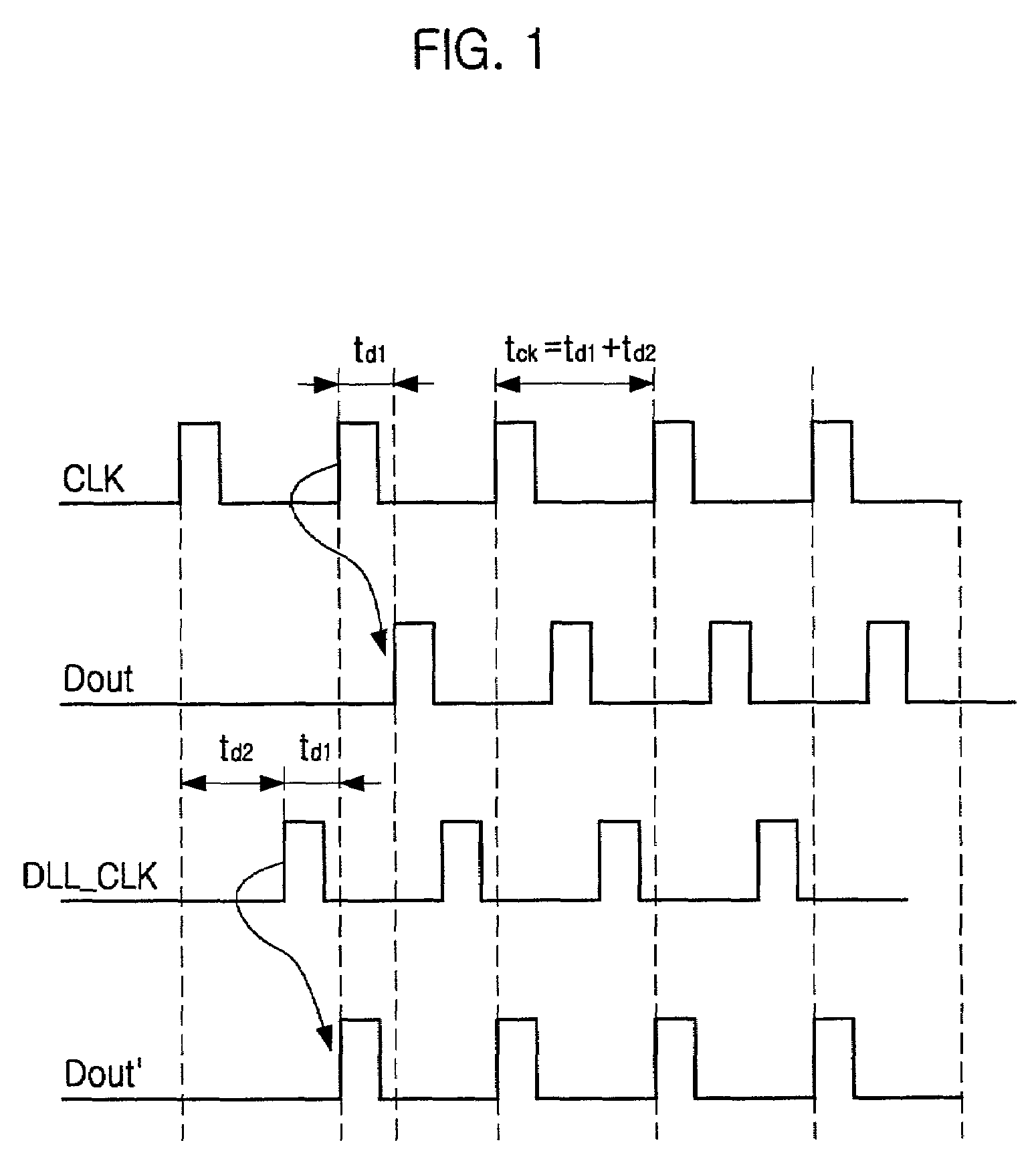
[0017]FIG. 1 is a timing chart for explaining a principle of a DLL. Here, tck denotes a time period of an external clock signal CLK.

[0018]As shown, when data is outputted in synchronization with the external clock signal CLK, a skew td1 between the external clock signal CLK and an output data Dout is caused. The skew td1 can be compensated by outputting the data in synchronization with an internal clock signal DLL_CLK that precedes the external clock signal CLK by the skew td1. At this time, the internal clock signal DLL_CLK is obtained by delaying the external clock signal CLK by a predetermined time td2 corresponding to (tck−td1). This, internal clock signal DLL_CLK is referred to as a DLL clock signal. Consequently, if the data is outputted in synchronization with the DLL clock signal, an output data Dout is synchronized with the external clock signal CLK.

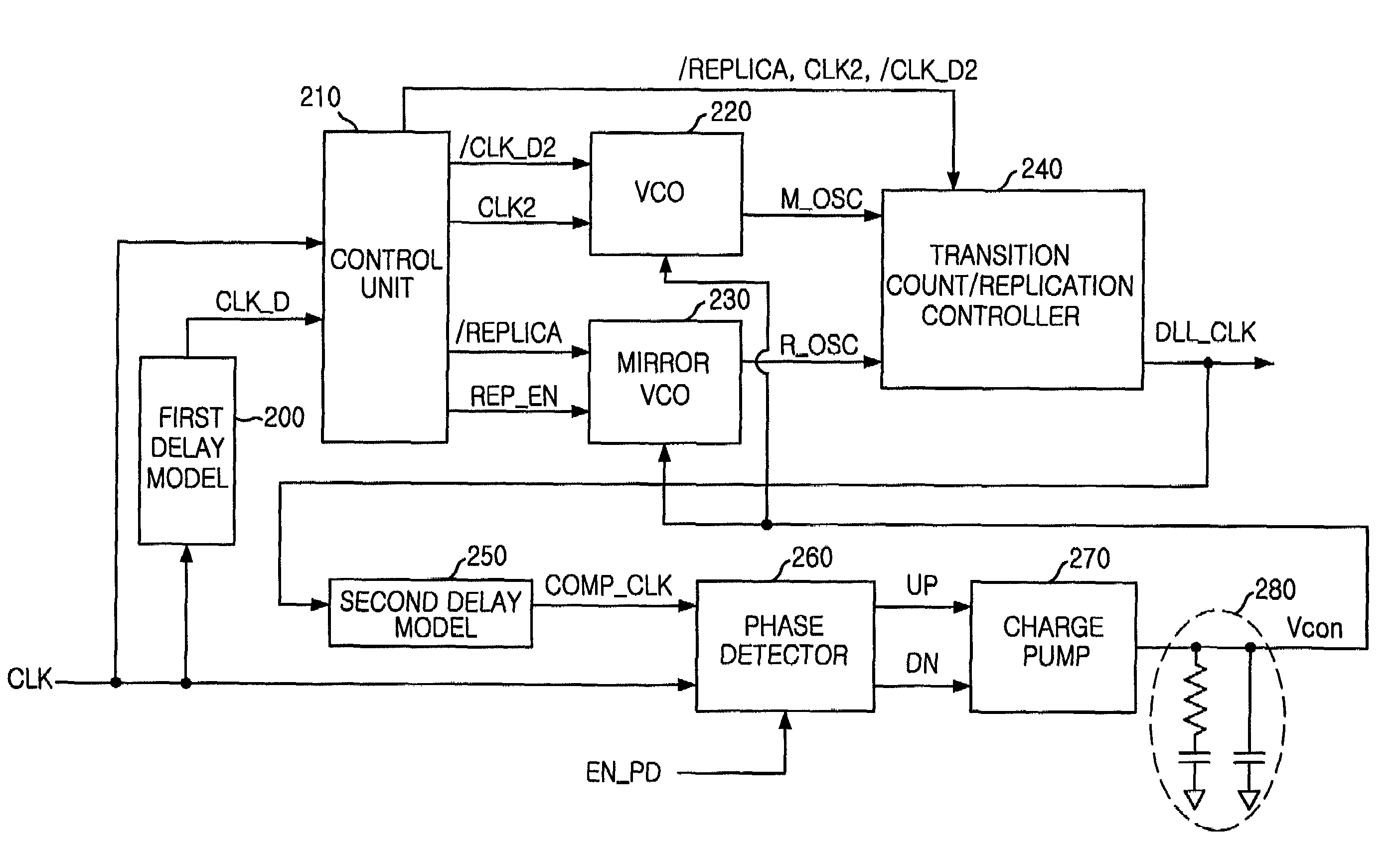
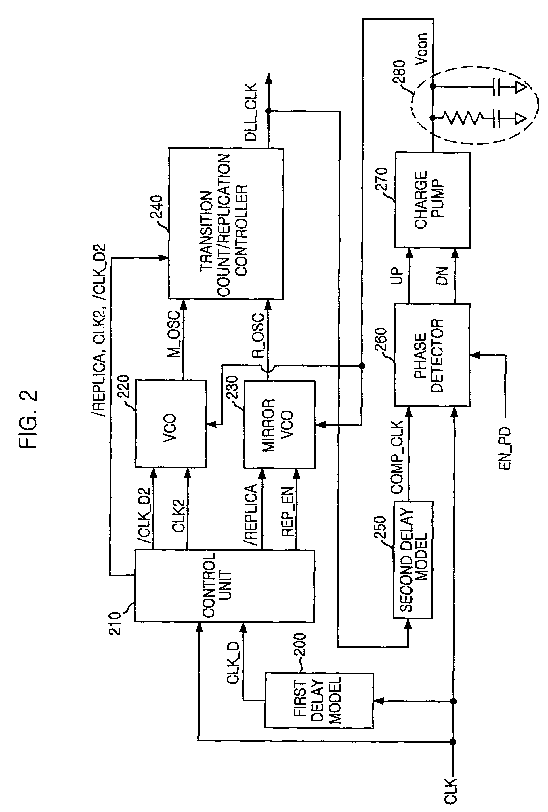
[0019]FIG. 2, is a block diagram illustrating a delay locked loop (DLL) in accordance with the present invention.

[0020]Referri...


PUM


Abstract

A delay locked loop (DLL) for compensating for a skew in a synchronous dynamic random access memory includes: a delay model means for delaying an external clock signal by the skew to generate a delayed clock signal; a control unit, in response to the external clock signal and the delayed clock signal, for generating control signals, wherein the control signal includes a control clock signal, a delayed control signal, a replication signal and a replication enable signal; a first voltage controlled oscillator, in response to the control clock signal and the delayed control signal, for generating a measurement oscillating signal; a second voltage controlled oscillator, in response to the replication signal and the replication enable signal, for generating a replication oscillating signal; a first unit, in response to the measurement oscillating signal and the replication oscillating signal, for generating a DLL clock signal; and a second unit for comparing a phase difference between the DLL clock signal and the external clock signal to generate a voltage control signal, wherein time periods of the measurement oscillating signal and the replication oscillating signal are changed by the voltage control signal.

Description

BACKGROUND OF THE INVENTION[0001]1. Field of the Invention[0002]The present invention relates to a semiconductor integrated circuit; and, more particularly, to a delay locked loop for use in synchronous dynamic random access memory, which is capable of obtaining a fast locking time and a reduced jitter.[0003]2. Description of the Prior Art[0004]For achieving a high speed operation in a semiconductor memory device, a synchronous dynamic access memory (SDRAM) has been developed. The SDRAM operates in synchronization with an external clock signal. The SDRAM includes a single data rate (SDR) SDRAM, a double data rate (DDR) SDRAM, and the like.[0005]Generally, when data are outputted in synchronization with the external clock signal, a skew between the external clock, signal and the output data is occurred. In the SDRAM, a delay locked loop (DLL) can be used to compensate for the skew between an external clock signal and an output data, or an external clock signal and an internal clock s...

Claims


Application Information

Patent Timeline
Patent Type & Authority Patents(United States)
IPC IPC(8): G11C8/00G11C7/00H03L7/00G11C7/22H03K5/135H03L7/089H03L7/099
CPCG11C7/22G11C7/222H03K5/135H03L7/0995H03L7/0891H03L7/00
Inventor LEE, SEONG HOON
Owner SK HYNIX INC
Why Eureka
Try Eureka