
Single event upset hardened circuitry without sensitivity to overshoot and/or undershoot conditions

a single event and hardened circuit technology, applied in logic circuits, pulse techniques, reliability increasing modifications, etc., can solve the problems of affecting the use of integrated circuits by terrestrial-based devices, affecting affecting the use of integrated circuits. , to achieve the effect of preventing the propagation of overshoot and undershoot conditions, preventing further propagation of overshoot conditions, and preventing undershoot conditions

Inactive Publication Date: 2007-05-08
HONEYWELL INT INC
View PDF3 Cites 7 Cited by
  • Summary
  • Abstract
  • Description
  • Claims
  • Application Information

AI Technical Summary

Benefits of technology

This solution effectively reduces the sensitivity of logic circuitry to SEE conditions, enhancing immunity to both overshoot and undershoot events, thereby improving the reliability and stability of integrated circuits in radiation-exposed environments without significant performance penalties.

Problems solved by technology

Along with these necessities, space, weight and cost limitations generally cause these integrated circuits to be very densely populated and highly complex.
As a consequence of operating in intergalactic space, earth orbital space, and high atmospheric altitudes, however, the integrated circuits are exposed to a large amount of radiation, which can effect their operation and, in turn, their reliability.
Recently, however, several radiation-laden atmospheric storms, which emanated from a coronal mass ejection of the sun, expanded into space, penetrated the Earth's magnetic field, and disrupted a significant amount of terrestrial-based devices that use integrated circuits.
When a radiation particle interferes with an integrated circuit, it can slow the circuit's performance and even upset circuit operation.
In Very Large Scale Integration (VLSI) circuits, radiation particles can also generate significant transient voltage and current disturbances on internal (e.g. power and ground) nodes.
The result of the flip-flopping of the states of the high-voltage-state and low-voltage-state nodes is that an output of the transistor, and in turn, a larger system into which the transistor is integrated (e.g., a logic gate) may undesirably change.
The consequence of having a temporary voltage disturbance on the transistor node, however, may be problematic because the SET condition may be propagated through the larger system.
Consequently, the contents of the data storage element are undesirably changed.
If, however, the data does not recover to the valid state before the latch closes, then the wrong data state may be loaded into the latch.
If this node is held in the opposite state for a period longer than a delay to trigger the logic circuit's next stage, then this next stage may undesirably switch states.
This unfortunately increases the size of logic circuit, which is often undesirable, particularly with data-storage elements that are duplicated many times over.
However, because the resistors increase the delay in a data storage circuit feedback loop, the time required to deliberately write the data storage circuit is also increased.
This is a significant performance penalty.
Another limitation of using cross-coupled resistors is that the material of choice is often polysilicon, often with a sheet resistance of about 100 k-ohm / square.
As known in the art, such radical changes are undesirable in a stable and reliable system.
In the past, increased write time increases were acceptable, but as the number of logic circuits (and the number of transistors thereof) proliferate, the resulting incremental write time increases are unacceptable from a system perspective.
Unfortunately, the cross-coupled transistors must typically be sufficiently “leaky” when turned “OFF” to function properly.
This bypass circuit and the previously discussed circuitry, however, may be sensitive to voltage overshoot and / or voltage undershoot conditions.
The consequences of such conditions can forward bias a diode and / or turn on one of the transistors in the bypass circuit, thereby undesirably performing the function of bypassing or shorting out the high resistance portion of the circuit.
Overshoot and undershoot conditions become more problematic as (i) technology scales down transistor feature sizes, (ii) diode forward bias voltages remain roughly constant, and (iii) transistor turn-on thresholds decrease below diode forward bias voltages.
As such, an overshoot or undershoot condition with a magnitude of a forward-bias-diode voltage drop can undesirably turn on the transistors.
This, in turn, reduces the logic circuitry's immunity to SEE conditions.

Method used


Image

  • Single event upset hardened circuitry without sensitivity to overshoot and/or undershoot conditions
  • Single event upset hardened circuitry without sensitivity to overshoot and/or undershoot conditions
  • Single event upset hardened circuitry without sensitivity to overshoot and/or undershoot conditions

Examples


Embodiment Construction

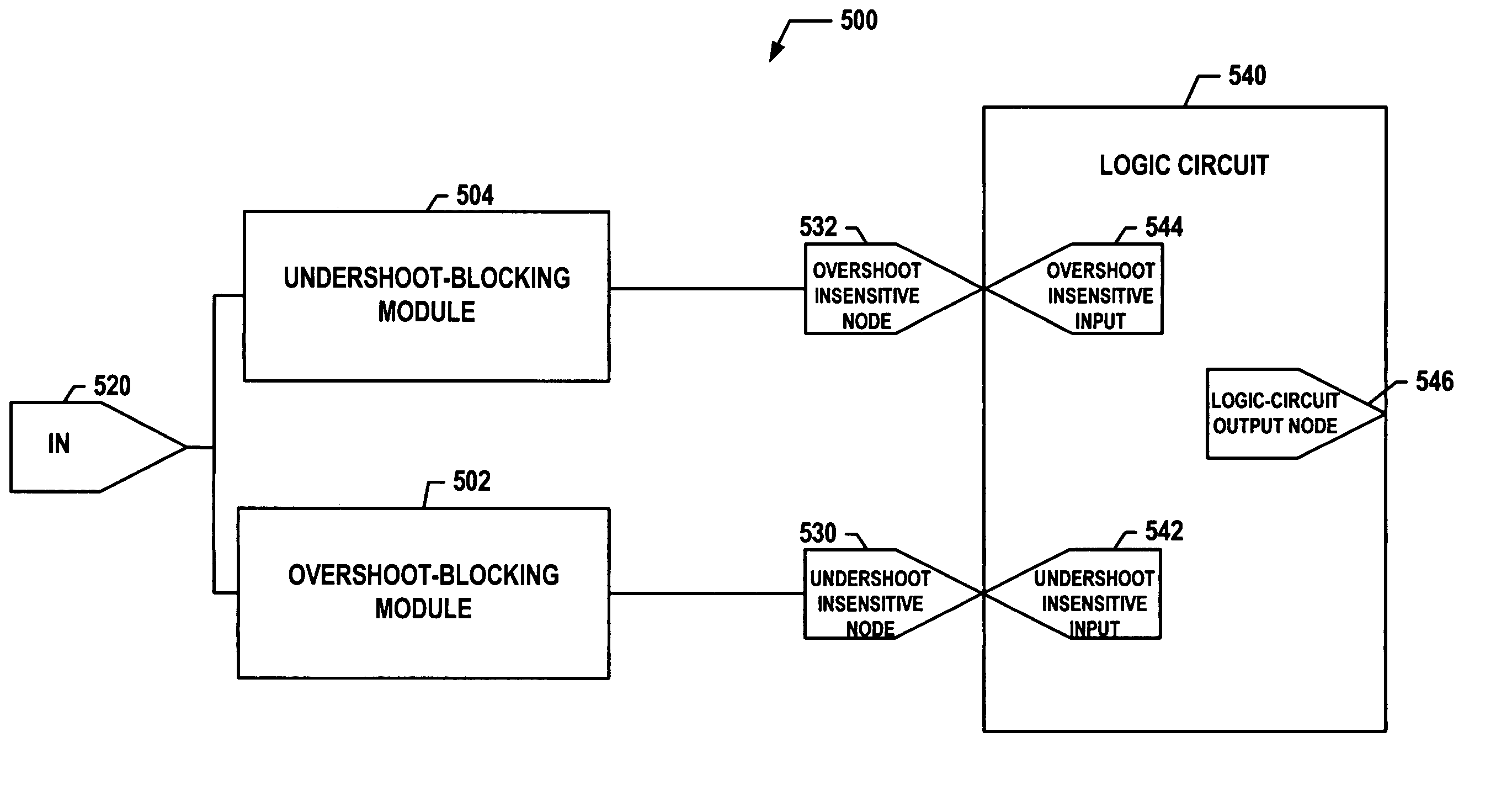
[0041]FIG. 5 is a block diagram illustrating an SEU hardening circuit 500 that provides immunity to voltage overshoot and / or undershoot conditions. The SEU hardening circuit 500 (or multiples thereof) may be placed between a first and second stage of a larger integrated or integral system.

[0042]As noted above, voltage overshoot and undershoot conditions may occur in integrated circuits due to radiation particles striking one or more “PN” junction regions of such integrated circuits. An overshoot condition can result from a radiation-particle strike that causes a voltage level on a node of the integrated circuit to exceed a nominal power voltage (e.g., a nominal VDD or a logic-1 level). Conversely, an undershoot condition can result from a radiation-particle strike that causes a voltage level on a node of the integrated circuit to fall below a nominal ground voltage (e.g., nominal VSS, Ground or a logic-0 level).

[0043]To provide immunity against such voltage overshoot and / or undersho...


PUM


Abstract

An apparatus for hardening logic circuitry against a Single-Event-Effect condition and for providing immunity to an overshoot and undershoot condition is provided. The apparatus includes undershoot-blocking and overshoot-blocking modules that are configured to be coupled to overshoot-insensitive and undershoot-insensitive nodes of the logic circuitry, respectively. The undershoot-blocking module is operable to (i) receive from a first node of the logic circuitry a first signal event having a undershoot condition impressed thereon, and (ii) block it from passing to the overshoot-insensitive node. The overshoot-blocking module is operable to (i) receive from the first node a second signal event having an overshoot condition impressed thereon, and (ii) block it from passing to the undershoot-insensitive node. As such, further propagation of the overshoot and undershoot conditions are prevented.

Description

BACKGROUND[0001]1. Field[0002]The following relates to integrated circuitry, and more particularly, to Single Event Effect (“SEE”) hardened circuitry for use with integrated circuitry, such as data storage circuitry. The following is directed toward reducing and / or eliminating the sensitivity of logic circuitry to SEE conditions, and to increasing the immunity of the logic circuitry to undershoot and / or overshoot conditions.[0003]2. Related Art[0004]Integrated circuits used in devices that operate in intergalactic space, earth orbital space, and high atmospheric altitudes (e.g., commercial flight altitudes) generally have to be highly reliable and operate using very low levels of power. Along with these necessities, space, weight and cost limitations generally cause these integrated circuits to be very densely populated and highly complex.[0005]As a consequence of operating in intergalactic space, earth orbital space, and high atmospheric altitudes, however, the integrated circuits ...

Claims


Application Information

Patent Timeline
Patent Type & Authority Patents(United States)
IPC IPC(8): H03K19/007H03K19/003
CPCH03K19/00338
Inventor CARLSON, ROY
Owner HONEYWELL INT INC
Learn More