Semiconductor device manufacturing method capable of reliable inspection for hole opening and semiconductor devices manufactured by method
- Summary
- Abstract
- Description
- Claims
- Application Information
AI Technical Summary
Benefits of technology
Problems solved by technology
Method used
Image
Examples
first embodiment
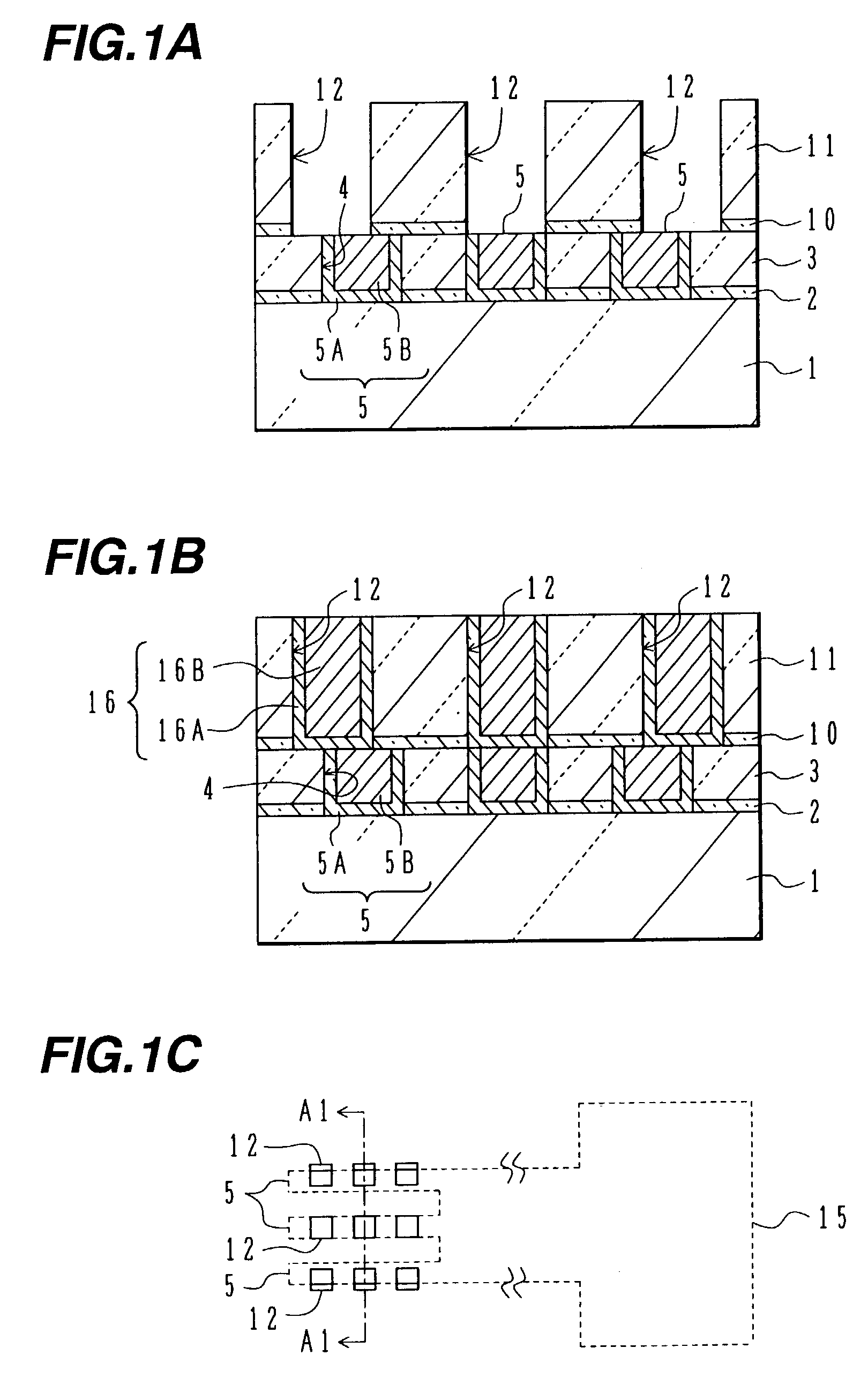
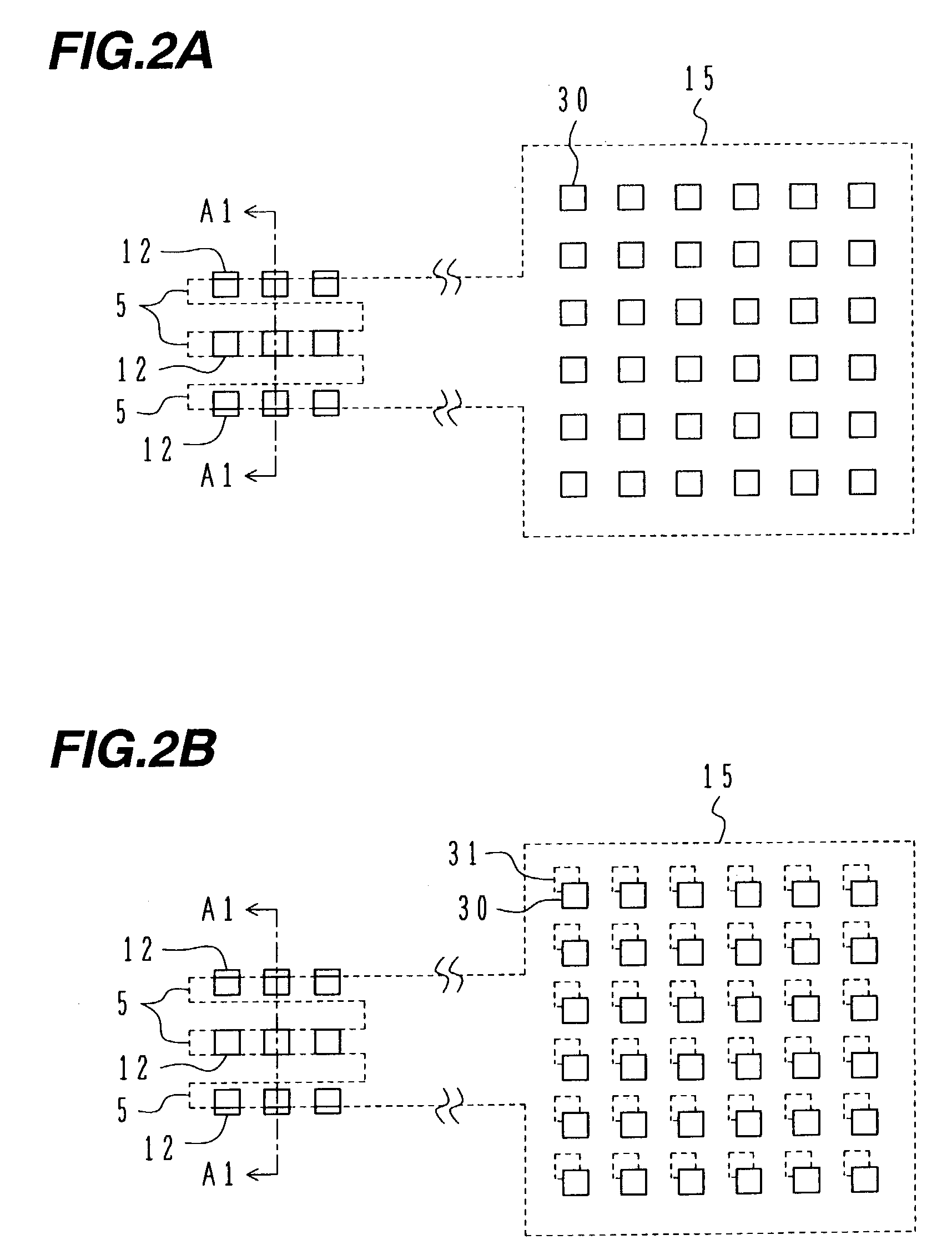
[0045]With reference to FIGS. 1A to 1C, a semiconductor device and its manufacturing method according to the invention will be described.
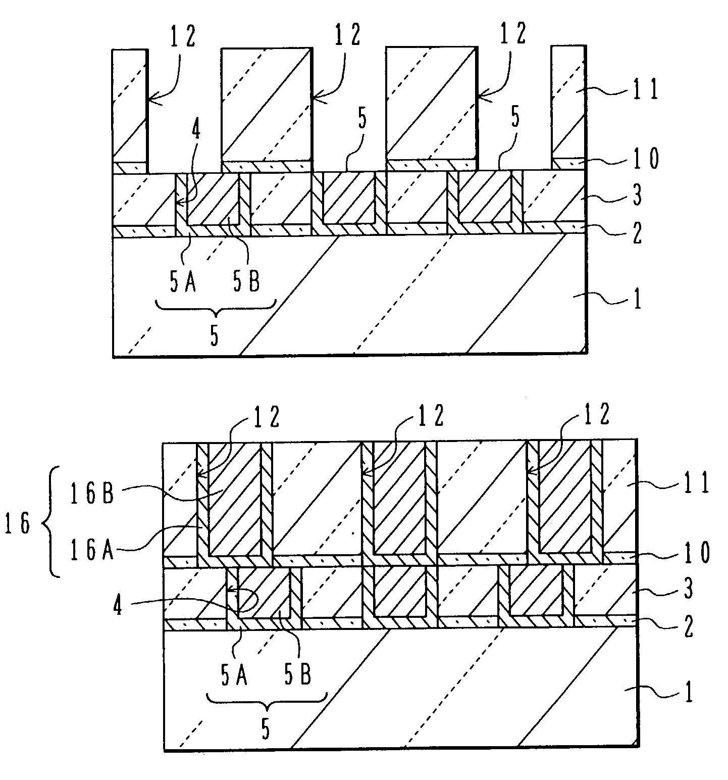
[0046]FIGS. 1A and 1B are cross sectional views of the peripheral area of via holes of a semiconductor device of the first embodiment. FIG. 1C is a schematic plan view of an inspection pattern for hole opening. The cross sectional views taken along one-dot chain line A1—A1 of FIG. 1C correspond to FIGS. 1A and 1B. Processes up to the state shown in FIG. 1A will be described.
[0047]On an interlayer insulating film 1 made of SiO2, an etching stopper film 2 of SiN having a thickness of 50 nm is formed by plasma CVD (plasma enhanced chemical vapor deposition). On the etching stopper film 2, a wiring layer insulating film 3 of SiO2 having a thickness of 500 nm is formed by plasma CVD.
[0048]On the surface of the wiring layer insulating film 3, a resist film is formed and openings corresponding to wiring grooves 4 are formed through the resist film. By usi...
second embodiment
[0067]In the second embodiment, even if the thickness of the interlayer insulating film 11 becomes irregular because of erosion, highly reliable inspection for hole opening is possible. In order to positively utilize erosion in the inspection wiring region 20, an area of the wiring lines in the inspection wiring region 20 is preferably set to 25% or higher of the area of the inspection wiring region 20. For example, the width W1 of each of the wring lines 5 and dummy wiring lines 5a is set to 0.2 μm and a distance between wiring lines is set to 0.6 μm.
[0068]If a depression to be formed by erosion is to be made deeper, for example, the wiring width W1 and distance S1 are both set to 1 μm, and the area of wiring lines in the inspection wiring region 20 is set to about 50% of the area of the inspection wiring region 20. The ratio of the area of wiring lines in the inspection wiring region 20 is set generally equal to the ratio of the area where opening is most difficult to be formed in...
third embodiment
[0069]FIGS. 5A and 5B are a cross sectional view and a plan view showing a semiconductor device according to the FIG. 5A corresponds to the cross sectional view taken along one-dot chain line A5—A5 shown in FIG. 5B.
[0070]In the first embodiment, the wiring pattern 5 is connected to the pad 15 as shown in FIG. 1C. In the third embodiment, a wiring pattern 5 is connected to an antimoisture ring 16. The antimoisture ring 16 is formed by the same process as that of forming the wiring pattern 5, and extends one turn along the outer peripheral area of the chip. The layout of the wiring pattern 5 and via holes 12 is similar to that of the semiconductor device of the first embodiment shown in FIGS. 1A and 1B.
[0071]An antimoisture ring groove 17 is formed through an interlayer insulating film 11 and an etching stopper film 10. The antimoisture ring groove 17 is formed by the same process as that of forming the via holes 12, and disposed on the underlying antimoisture ring 16.
[0072]In the th...
PUM
 Abstract
Description
Claims
Application Information
 - R&D
- Intellectual Property
- Life Sciences
- Materials
- Tech Scout
- Unparalleled Data Quality
- Higher Quality Content
- 60% Fewer Hallucinations
Browse by: Latest US Patents, China's latest patents, Technical Efficacy Thesaurus, Application Domain, Technology Topic, Popular Technical Reports.
© 2025 PatSnap. All rights reserved.Legal|Privacy policy|Modern Slavery Act Transparency Statement|Sitemap|About US| Contact US: help@patsnap.com


