Semiconductor switching device

a switching device and semiconductor technology, applied in electronic switching, waveguide type devices, pulse techniques, etc., can solve the problems of reducing the maximum power allowed to pass through the switching device and insufficient maximum power to transmit signals

Inactive Publication Date: 2007-04-17
SEMICON COMPONENTS IND LLC
View PDF24 Cites 3 Cited by
  • Summary
  • Abstract
  • Description
  • Claims
  • Application Information

AI Technical Summary

Benefits of technology

[0028]On the off side, the FET used for receiving signals, which is turned off during signal transmission by the other FET, has to withstand the voltage required for generating the allowed maximum power of the FET used for transmitting signals while the FET is transmitting signals. This can be accomplished by lowering the pinch-off voltage of the FET on the off side, as will be later described in detail. In general, the pinch-off voltage of FET can be lowered by reducing the depth of the channel layer or the impurity concentration of the channel layer.

Problems solved by technology

However, further reduction of the gate width results in a reduction of the maximum power allowed to pass through the switching device.
This maximum power is not enough to transmit signals when the switching device is used in a system conforming to the BLUETOOTH or Wireless LAN standard.

Method used


Image

  • Semiconductor switching device
  • Semiconductor switching device
  • Semiconductor switching device

Examples


Embodiment Construction

[0021]An embodiment of this invention will be described hereinafter with reference to the FIGS. 2–9.

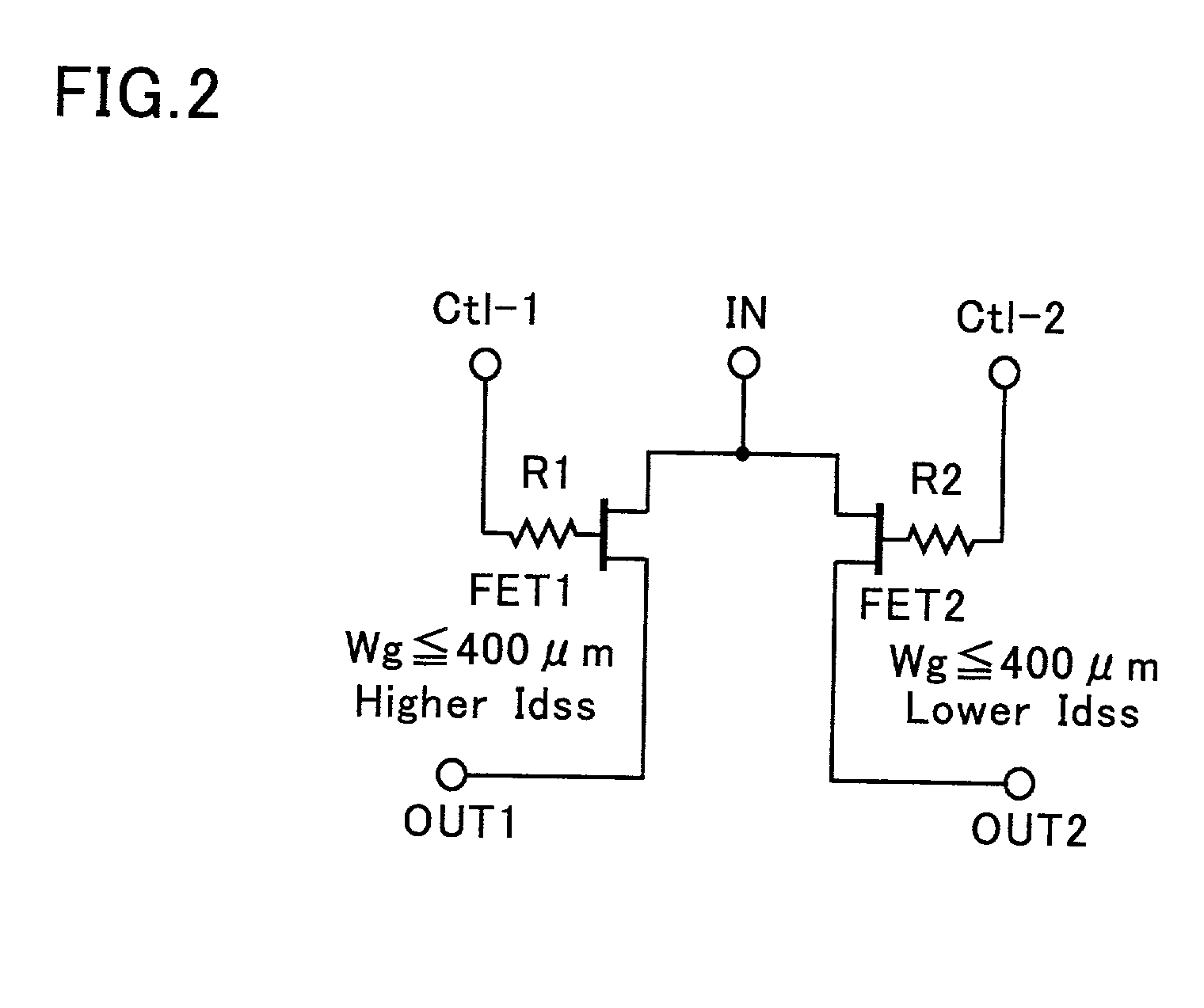
[0022]FIG. 2 is a circuit diagram of a semiconductor switching circuit device of an embodiment of this invention, which preferably operates at a frequency of 2.4 GHz or higher. The device has first and second FETs (FET1, FET2), each of which has a source electrode, a gate electrode and a drain electrode on its channel layer. The device also has a common input terminal IN connected to the source electrodes (or the drain electrodes) of the FETs (FET1, FET2), a first output terminal connected to the drain electrode (or the source electrode) of the first FET (FET1), and a second output terminal connected to the drain electrode (or the source electrode) of the second FET (FET2). The gate electrode of FET1 is connected to a control terminal Ctl-1 via resistor R1, and the gate electrode of FET2 is connected to a control terminal Ctl-2 via resistor R2. A pair of complementary signals is appli...


PUM


Abstract

A semiconductor switching device includes two FETs with different device characteristics, a common input terminal, and two output terminals. The gate width of each FET is about 400 μm, and the maximum power required for the device operation is maintained by a lager conductivity of the channel layer of one FET and by a lower conductivity of the channel layer of another FET. The device operates at frequencies of 2.4 GHz or higher without use of shunt FET.

Description

BACKGROUND OF THE INVENTION[0001]1. Field of the Invention[0002]The invention relates to a semiconductor switching device for switching at high frequencies, especially to a compound semiconductor switching device operating at frequencies equal to or higher than 2.4 GHz.[0003]2. Description of the Related Art[0004]Mobile communication devices such as mobile telephones often utilize microwaves in the GHz range, and commonly need switching devices for high frequency signals which are used in switching circuits for changing antennas and switching circuits for transmitting and receiving such signals. A typical example of such a switching device can be found in Japanese Laid-Open Patent Application No. Hei 9-181642. Such a device often uses a field-effect transistor (called FET hereinafter) formed on a gallium arsenide (GaAs) substrate, as this material is suitable for use at high frequencies, and developments have been made in forming a monolithic microwave integrated circuit (MMIC) by i...

Claims


Application Information

Patent Timeline
Patent Type & Authority Patents(United States)
IPC IPC(8): H04B1/44H01L29/06H01L31/00H01L27/095H01L27/06H01L29/80H01L29/812H01P1/15H03K17/16
CPCH01L27/0605H01L29/812H01L29/80
Inventor ASANO, TETSUROHIRAI, TOSHIKAZU
Owner SEMICON COMPONENTS IND LLC
Why Eureka
Try Eureka