
Method for fabricating ferroelectric capacitor

a technology of ferroelectric capacitors and capacitors, which is applied in the direction of capacitors, semiconductor devices, electrical equipment, etc., can solve the problems of small top electrodes compared to design values, and the obstacle to improve the integration degree, and achieve the effect of high integration and wide-area top electrodes

Inactive Publication Date: 2007-04-03
FUJITSU SEMICON LTD
View PDF5 Cites 6 Cited by
  • Summary
  • Abstract
  • Description
  • Claims
  • Application Information

AI Technical Summary

Benefits of technology

"The present invention provides a method for making a ferroelectric capacitor that allows for easy formation of a highly-integrated and wide-area top electrode. The method involves sequentially adding layers of a first conductive film, a ferroelectric film, and a second conductive film onto a base film. The second conductive film is then shaped into a rectangular planar shape by etching it twice or more using different masks. The first mask is used to create a portion of the top electrode that is parallel to the sides of the rectangle, while the second mask is used to create another portion of the top electrode that is perpendicular to the first direction. This method simplifies the process of making a ferroelectric capacitor and allows for easier integration of multiple layers."

Problems solved by technology

However, in such a conventional fabricating method, as described above, there are generated curbed portions at the four corners of the resist mask 111 intended for etching a top electrode, causing the top electrode to be small as compared to the design value.
Such a loss of area becomes remarkable as the integration degree is improved to thereby downsize the top electrode in the future, so that the loss results in an obstacle to improve the integration degree.

Method used


Image

  • Method for fabricating ferroelectric capacitor
  • Method for fabricating ferroelectric capacitor
  • Method for fabricating ferroelectric capacitor

Examples


Embodiment Construction

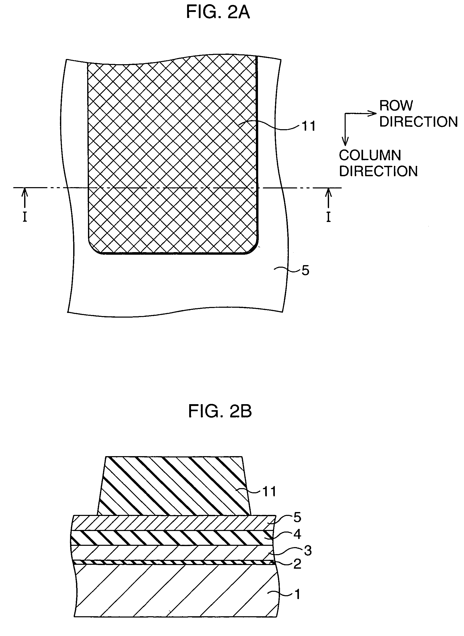
[0029]Hereinafter, an embodiment according to the present invention will be described specifically with reference to the attached drawings. FIGS. 1A and 1B to FIGS. 6A and 6B are views showing a method for fabricating a ferroelectric memory having a ferroelectric capacitor according to the present invention. Here, FIGS. 1A, 2A, 3A, 4A, 5A and 6A are top views, and FIGS. 1B, 2B, 3B, 4B, 5B and 6B are sectional views showing sections taken along the I—I lines in FIGS. 1A, 2A, 3A, 4A, 5A and 6A, respectively. In addition, FIGS. 7A and 7B are sectional views showing a configuration of a memory cell of the ferroelectric memory. FIG. 8 is a layout showing the relation between electrodes, and FIGS. 7A and 7B correspond to sectional views showing sections taken along the III—III line and the IV—IV line in FIG. 8, respectively.

[0030]In the present embodiment, as a memory, a ferroelectric memory in which planar-type memory cells each having 1T1C (a single transistor and a single capacitor) ar...


PUM


Abstract

A method for fabricating a ferroelectric memory having memory cells arranged in arrays, wherein an Al2O3 film (2), a Pt film (3), a PZT film (4) and IrO2 film (5) are formed on an interlayer insulation film. At the time of forming a top electrode, the IrO2 film (5) is patterned using a resist mask having a part extending in the row direction, and then patterned using a resist mask having a part extending in the column direction. Consequently, a top electrode of the IrO2 film (5) having a rectangular plan view is formed at the intersection of these resist masks.

Description

[0001]This application is a continuation of international application PCT / JP03 / 02212 filed on Feb. 27, 2003.TECHNICAL FIELD[0002]The present invention relates to a method for fabricating a ferroelectric capacitor suitable for a ferroelectric memory and so forth.BACKGROUND ART[0003]In a ferroelectric memory, plural pieces of memory cells are arranged in a matrix form, and each one of the memory cells is provided with a ferroelectric capacitor. Further, the ferroelectric capacitors are divided into those of a stack type and those of a planar type, of which the planar-type ferroelectric capacitor sometimes has a plate line commonly used for a group of top electrodes in plural lines.[0004]FIGS. 10A and 10B to FIGS. 13A and 13B are views showing a conventional method for fabricating a ferroelectric capacitor in the order of steps. Here, the FIGS. 10A, 11A, 12A, and 13A are top views, and FIGS. 10B, 11B, 12B, and 13B are sectional views taken along the I—I line in FIGS. 10A, 11A, 12A, and...

Claims


Application Information

Patent Timeline
Patent Type & Authority Patents(United States)
IPC IPC(8): H01L21/00H01L21/02H01L21/033H01L21/3213H01L21/8246H01L27/105H01L27/115
CPCH01L21/32139H01L27/11502H01L27/11507H01L28/65H01L21/0334H01L21/32136H01L28/55H10B53/30H10B53/00
Inventor OKITA, YOICHI
Owner FUJITSU SEMICON LTD
Learn More