Submount and semiconductor device
a semiconductor device and sub-mount technology, applied in the direction of semiconductor lasers, semiconductor/solid-state device details, soldering apparatus, etc., can solve the problems of reduced density of solder layer, preventing adequate improvement of bonding strength, and density greater than 99.9% of the theoretical density,
- Summary
- Abstract
- Description
- Claims
- Application Information
AI Technical Summary
Benefits of technology
Problems solved by technology
Method used
Image
Examples
first embodiment
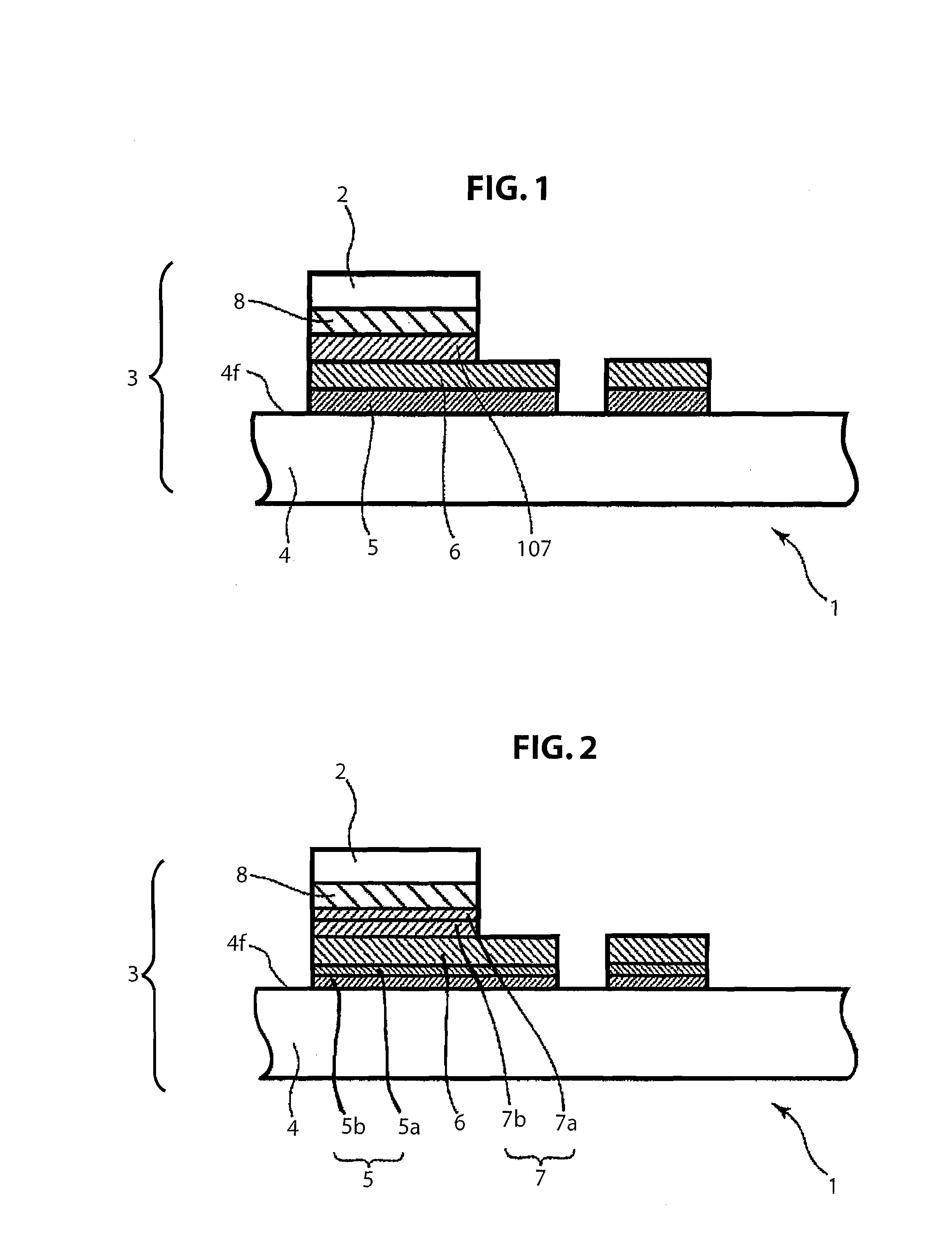
[0028]An embodiment of the present invention will be described, with references to the figures. Elements that are identical or correspond to each other in these figures are assigned the same numerals and overlapping descriptions will be omitted. FIG. 1 shows a simplified cross-section drawing of a semiconductor device according to the first embodiment of the present invention. As shown in FIG. 1, the semiconductor device 1 is equipped with: a submount 3; and a laser diode 2, serving as a semiconductor light-emitting element, mounted on the submount 3 via a solder layer 8. The solder layer 8 has a density of at least 50% and no more than 99.9% of the theoretical density of the AuSn-based solder used in the solder layer 8.
[0029]The submount 3 is formed by layering the following onto a substrate 4: a Ti / Pt layered film 5; a gold (Au) film 6; a solder barrier layer 107; and a solder layer 8. The semiconductor device shown in FIG. 1 is made by first preparing the submount 3 onto which th...
second embodiment
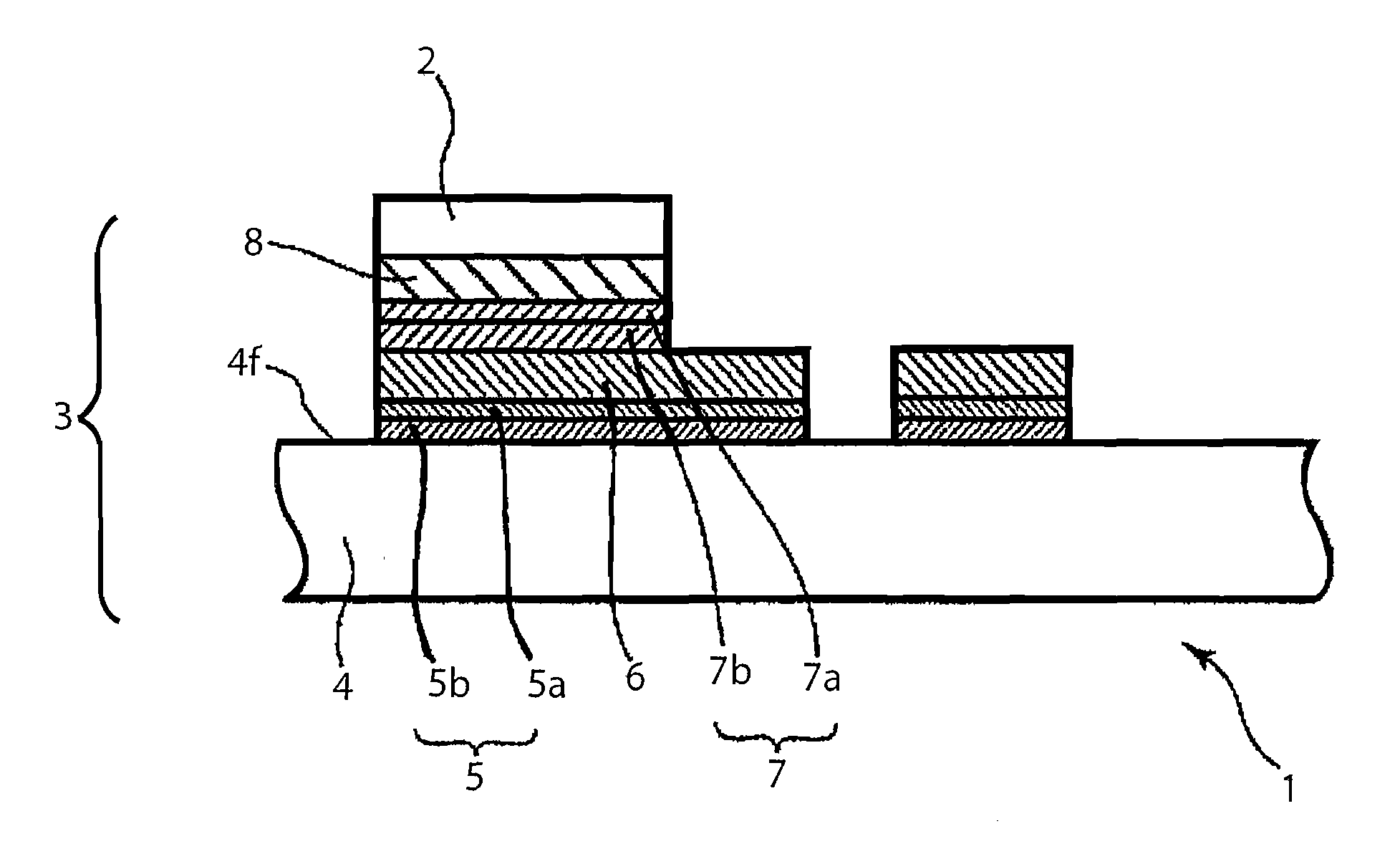
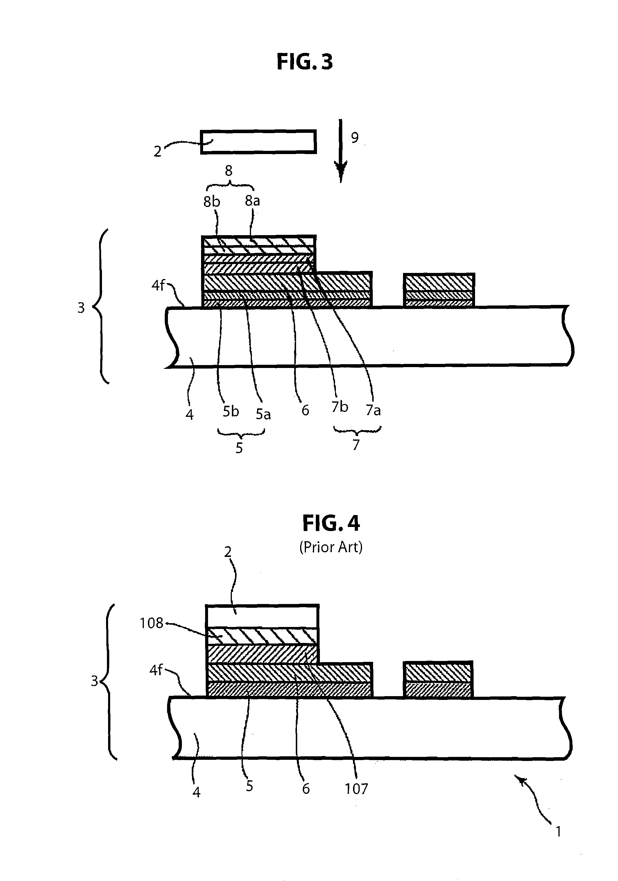
[0034]FIG. 2 shows a simplified cross-section drawing of a semiconductor device according to a second embodiment of the present invention. FIG. 3 is a simplified cross-section drawing for the purpose of describing how the semiconductor device shown in FIG. 2 is made, and shows the state before solder is melted.
[0035]As shown in FIG. 2, the semiconductor device 1 is formed as a structure wherein a laser diode 2 serving as a semiconductor light-emitting element is mounted onto a submount 3. The submount is formed from: a submount substrate 4 formed from a material such as sintered aluminum nitride (AlN); a layered film 5 (Ti / Pt layered film 5) formed from a titanium (Ti) film 5b serving as an adhesion layer and a platinum (Pt) film 5a serving as a diffusion barrier layer; a gold (Au) film 6 formed on the Ti / Pt layered film 5 and serving as an electrode layer; and a solder adhesion layer 7 formed from a titanium (Ti) film 7b serving as a transition element layer and a platinum (Pt) fil...
embodiment
(Making and Evaluating Samples)
[0068]Based on the method described above, submounts were made from sample 1 through sample 11 indicated in Table 1. Samples 2 through 11 correspond to embodiments and sample 1 corresponds to a comparative example.
[0069]
TABLE 1Solder LayerSolderSolderSolderfilm-Laser diodecompositionSolder filmrelativeformationDie ShearSampleratio (massthicknessdensityrateBondingstrengthNumberSubstrateratio)(microns)(%)(nm / s)temperature(MPa)1SinteredAg:Sn = 32:681.5 / 4.042125037AIN(layered Ag / Sn)2SinteredAg:Sn = 32:681.5 / 4.0621.525047AIN(layered Ag / Sn)3SinteredAg:Sn = 32:681.5 / 4.099225052AIN(layered Ag / Sn)4SinteredAg:Sn = 32:681.5 / 4.092525051AIN(layered Ag / Sn)5SinteredAg:Sn = 32:681.5 / 4.088925050AIN(layered Ag / Sn)6SinteredAg:Sn = 32:681.5 / 4.094225049SiC(layered Ag / Sn)7SinteredAg:Sn = 32:681.5 / 4.095225047Al2O3(layered Ag / Sn)8CuWAg:Sn = 32:681.5 / 4.097225048(layered Ag / Sn)9SinteredAg:Sn = 10:903.5 (alloy)96225049AIN10SinteredAu:Sn = 80:203.5 (alloy)93228547AIN11SinteredAu:...
PUM
| Property | Measurement | Unit |
|---|---|---|
| flatness | aaaaa | aaaaa |
| flatness | aaaaa | aaaaa |
| thickness | aaaaa | aaaaa |
Abstract
Description
Claims
Application Information
 - R&D
- Intellectual Property
- Life Sciences
- Materials
- Tech Scout
- Unparalleled Data Quality
- Higher Quality Content
- 60% Fewer Hallucinations
Browse by: Latest US Patents, China's latest patents, Technical Efficacy Thesaurus, Application Domain, Technology Topic, Popular Technical Reports.
© 2025 PatSnap. All rights reserved.Legal|Privacy policy|Modern Slavery Act Transparency Statement|Sitemap|About US| Contact US: help@patsnap.com


