
Polishing composition and method for forming wiring structure using the same

a technology of coating composition and wiring structure, which is applied in the direction of detergent composition, other chemical processes, manufacturing tools, etc., can solve the problems of degrading the electrical characteristics surface defects of the semiconductor device,

Inactive Publication Date: 2007-03-13
FUJIMI INCORPORATED
View PDF24 Cites 10 Cited by
  • Summary
  • Abstract
  • Description
  • Claims
  • Application Information

AI Technical Summary

Benefits of technology

[0006]An object of the present invention is to provide a polishing composition capable of satisfactorily polishing a semiconductor device.

Problems solved by technology

The remaining iron ions cause surface defects to occur in the semiconductor device and degrade electrical characteristics of the semiconductor device.
Therefore, the second conventional polishing composition does not inhibit erosion.

Method used


Image

  • Polishing composition and method for forming wiring structure using the same
  • Polishing composition and method for forming wiring structure using the same
  • Polishing composition and method for forming wiring structure using the same

Examples


examples

[0115]The present invention will now be more specifically described with Examples and Comparative Examples.

examples 27 to 39

[0118]In Examples 27 to 29, fumed silica, periodic acid, hydrochloric acid, tetramethyl ammonium hydroxide and water were mixed to prepare a polishing composition. The average particle size D1 and the average particle size D2 of fumed silica contained in the polishing compositions prepared in Examples 27 to 39 are shown in Table 2. The content of fumed silica in polishing compositions prepared in Examples 27 to 39 is 100 gAiter, the content of periodic acid is 20 g / liter, the mass fraction of chlorine is 100 ppm, and the content of tetramethyl ammoniun hydroxide is a content allowing the polishing composition to be kept at pH of 2.3.

[0119]Using polishing compositions prepared in Examples 1 to 39 and Comparative Examples 1 to 5, a blanket wafer of tungsten and a blanket wafer of SiO2 were polished for 1 minute in accordance with polishing conditions (1) described below. At this time, the tungsten polishing rate and the SiO2 polishing rate of each polishing composition was determined ...

examples 40 to 58

[0125]In Examples 40 to 58, a pattern wafer was polished for 1 minute in accordance with the above polishing conditions (1) using the polishing composition prepared in Example 4, and then finish-polished using a finish-polishing composition in accordance with the polishing conditions (2) described below. Alter the pattern wafer was finish-polished, the amount of dishing and the amount of erosion in an area of the pattern wafer having a density of 50% and a hole diameter of 1 μm, namely the area of the pattern wafer on which wiring portions relatively densely, where measured. The results are shown in Table 3 below. The finish-polishing composition used in each Example was prepared by mixing colloidal silica, periodic acid, ammonia and water. The contents of colloidal silica and periodic acid in the finish-polishing composition and the pH of the finish-polishing are shown in Table 3 below. In addition, the tungsten polishing rate and SiO2 polishing rate of the finish-polishing composi...


PUM

PropertyMeasurementUnit
particle sizeaaaaaaaaaa

Abstract

A polishing composition capable of satisfactorily polishing a semiconductor. The first polishing composition of the present invention includes silicon dioxide, at least one component selected from periodic acids and salts thereof, at least one component selected from tetraalkyl ammonium hydroxides and tetraalkyl ammonium chlorides, hydrochloric acid, and water, and contains substantially no iron. The second polishing composition of the present invention includes a predetermined amount of fumed silica, a predetermined amount of at least one component selected from periodic acids and salts thereof, a tetraalkyl ammonium salt represented by the following general formula (1), at least one component selected from ethylene glycol and propylene glycol, and water. The pH of the second polishing composition is greater than or equal to 1.8 and is less than 4.0.

Description

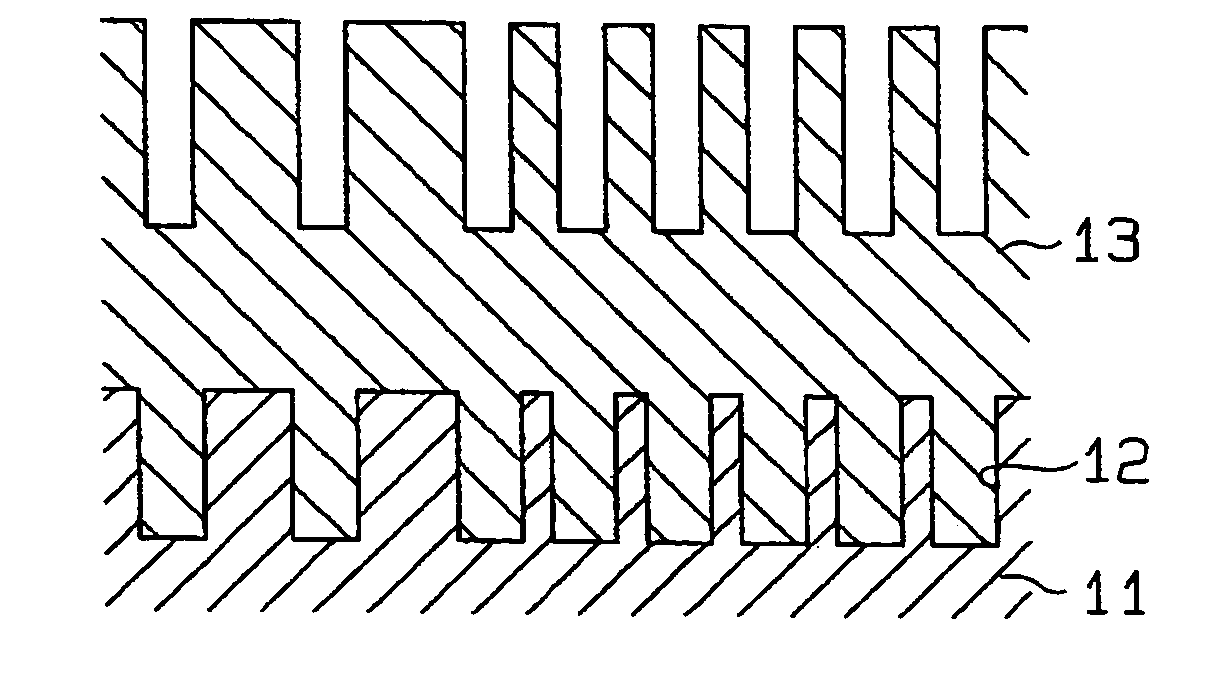
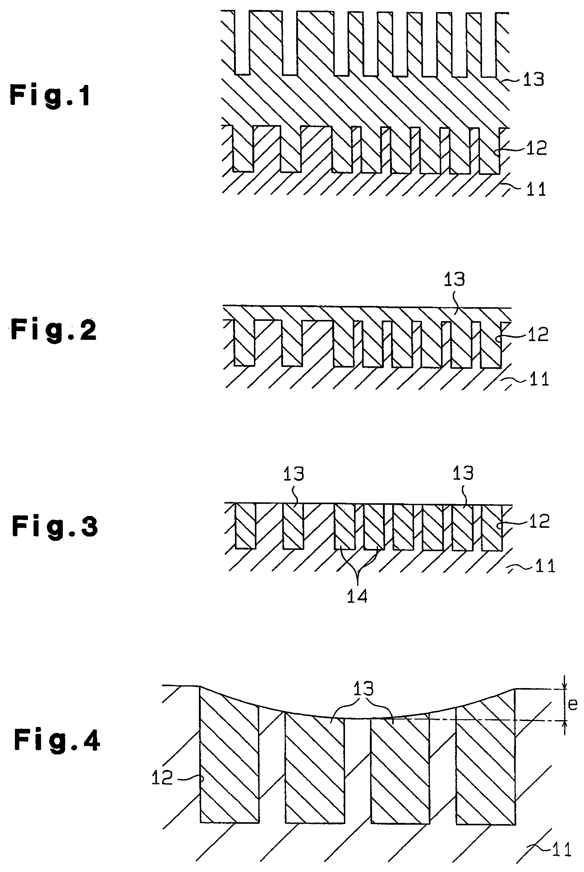
FIELD OF THE INVENTION[0001]The present invention relates to a polishing composition for use in formation of a wiring structure in, for example, a semiconductor device, and a method for forming a wiring structure using the polishing composition.BACKGROUND OF THE INVENTION[0002]A polishing composition for use in formation of a wiring structure in a semiconductor device is required to have a high capability for polishing a conductive metal such as tungsten and have a low capability for polishing an insulator such as silicon dioxide. This is intended for inhibiting the occurrence of erosion on the surface of the semiconductor device.[0003]For forming the wiring structure, a conductor layer 13 composed of a conductive metal is generally formed on an insulator layer 11 having trenches 12 on the surface (see FIG. 1). Thereafter, the conductor layer 13 is polished so that the insulator layer 11 in areas other than trenches 12 is exposed (see FIG. 3). Erosion refers to a phenomenon in which...

Claims


Application Information

Patent Timeline
Patent Type & Authority Patents(United States)
IPC IPC(8): C09K13/00C09G1/02C09K3/14H01L21/321
CPCC09G1/02H01L21/3212C09K3/1463C09K3/14
Inventor OHNO, KOJIHORIKAWA, CHIYOSAKAI, KENJITAMAI, KAZUSEIINA, KATSUYOSHI
Owner FUJIMI INCORPORATED
Learn More