RFID tag reading system and method
a technology of radio frequency identification and tag reading, applied in the field of position determination and tracking systems, can solve the problems of reducing the range over which readers may communicate with tags, current available tags are relatively expensive, and available tags consume large amounts of power
- Summary
- Abstract
- Description
- Claims
- Application Information
AI Technical Summary
Benefits of technology
Problems solved by technology
Method used
Image
Examples
first embodiment
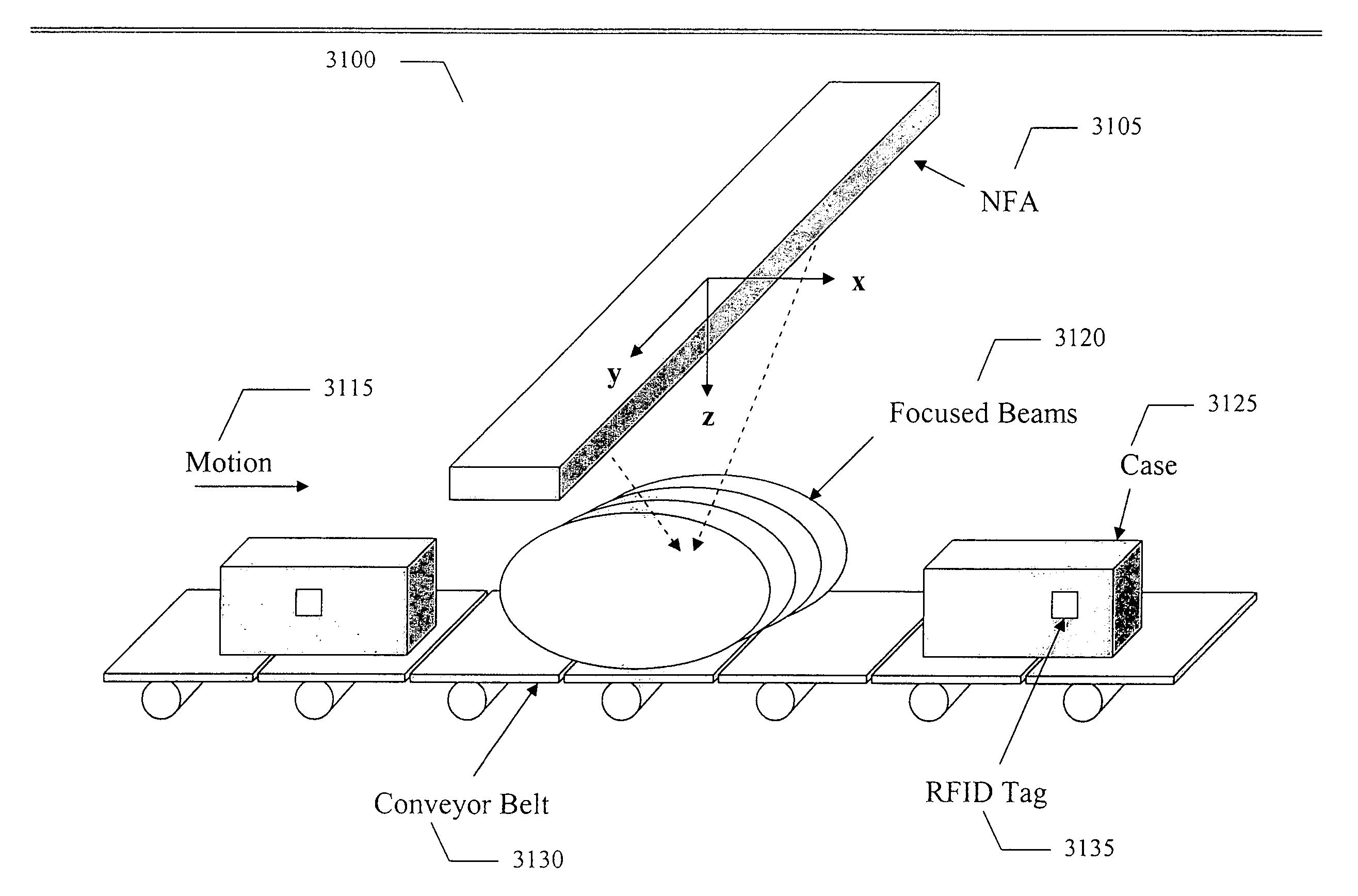
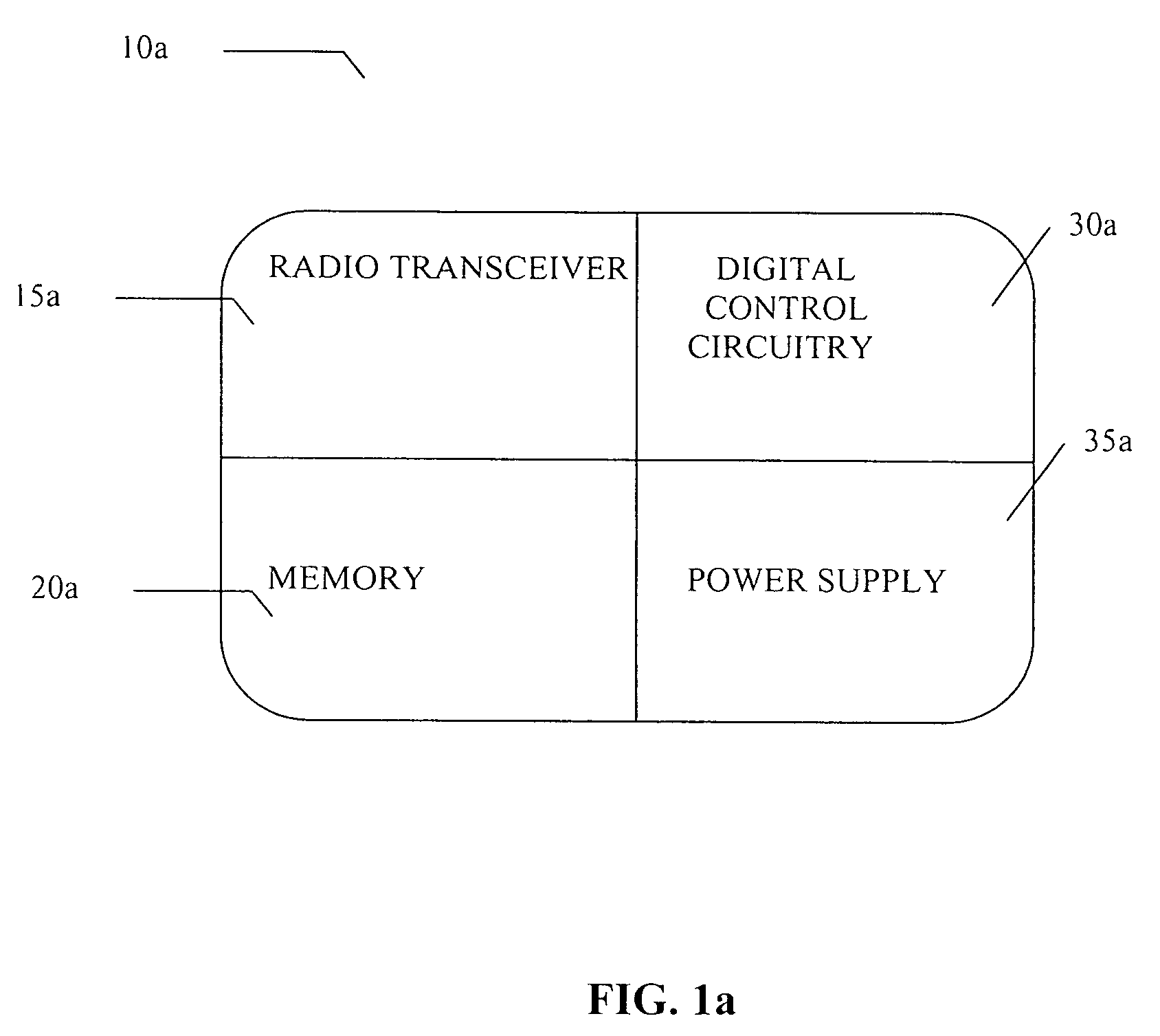
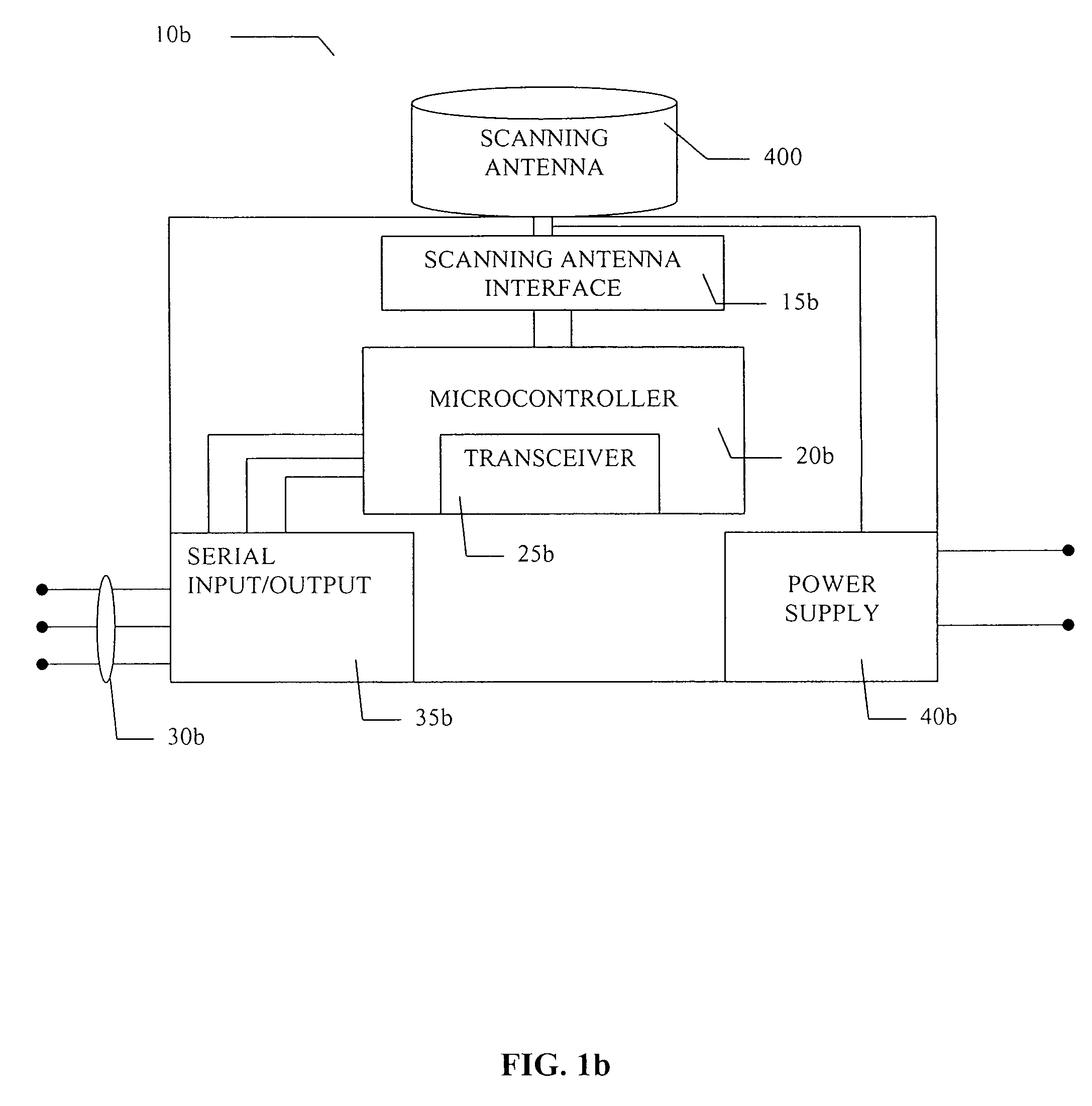
[0066]The present invention serves as an internal or external antenna for a RF ID TAG reader application as well as a position determination and tracking system and method. The antenna interfaces with an RFID reader that can be used in a RF ID tag system for significant performance advantages. The antennas described herein can operate in any one, all or part of the following frequencies: the 2.4 GHz GHz Industrial, Scientific and Medical (ISM) band; the 5.1 to 5.8 GHz band; the 860–960 MHz band; or the 433 MHz band; although it is understood that they can operate in other bands as well. A software driver functions to control the antenna azimuth scan angle to maximize the received wireless signal from a tag associated with a reader. In a first embodiment, the key performance requirement to steer a beam with 6 dBi of gain throughout a 360° azimuth, or any segmentation of 360 degrees, scan is enabled.
[0067]Existing RF ID TAG READERS currently use fixed antennas. For lower frequency sys...
second embodiment
[0150]Referring to FIG. 17, there is a perspective view that illustrates the basic components of the array antenna 1102b. The array antenna 1102b has a similar structure and functionality to array antenna 1102a except that the antenna elements 1702 and 1704 are configured as dipole elements instead of a monopole elements as shown in FIG. 12. The array antenna 1102b includes a radiating antenna element 1702 capable of transmitting and receiving radio signals and one or more parasitic antenna elements 1704 that are incapable of transmitting or receiving radio signals. Each parasitic antenna element 1704 (six shown) is located a predetermined distance away from the radiating antenna element 1702. A voltage-tunable capacitor 1706 (six shown) is connected to each parasitic element 1704. A controller 1708 is used to apply a predetermined DC voltage to each one of the voltage-tunable capacitors 1706 in order to change the capacitance of each voltage-tunable capacitor 1706 and thus enable o...
third embodiment
[0152]Referring to FIG. 18, there is a perspective view that illustrates the basic components of the array antenna 1102c. The array antenna 1102c includes a radiating antenna element 1002 capable of transmitting and receiving dual band radio signals. The array antenna 1102c also includes one or more low frequency parasitic antenna elements 1804a (six shown) and one or more high frequency parasitic antenna elements 1804b (six shown). The parasitic antenna elements 1804a and 1804b are incapable of transmitting or receiving radio signals. Each of the parasitic antenna elements 1804a and 1804b are locate a predetermined distance away from the radiating antenna element 1802. As shown, the low frequency parasitic antenna elements 1804a are located on a circumference of a “large” circle around both the radiating antenna element 1802 and the high frequency parasitic antenna elements 1804b. And, the high frequency parasitic antenna elements 1804b are located on a circumference of a “small” c...
PUM
 Abstract
Description
Claims
Application Information
 - R&D
- Intellectual Property
- Life Sciences
- Materials
- Tech Scout
- Unparalleled Data Quality
- Higher Quality Content
- 60% Fewer Hallucinations
Browse by: Latest US Patents, China's latest patents, Technical Efficacy Thesaurus, Application Domain, Technology Topic, Popular Technical Reports.
© 2025 PatSnap. All rights reserved.Legal|Privacy policy|Modern Slavery Act Transparency Statement|Sitemap|About US| Contact US: help@patsnap.com


