Register access scheduling method for multi-bank register file of a super-scalar parallel processor

Inactive Publication Date: 2007-02-13
SEMICON TECH ACADEMIC RES CENT
View PDF2 Cites 4 Cited by
  • Summary
  • Abstract
  • Description
  • Claims
  • Application Information

AI Technical Summary

Benefits of technology

[0015]It is an objective of the present invention to provide a parallel processor which can incorporate a multi-bank register file by arbitrating the execution timings of input instructions and devising the configuration of the multi-bank register file, can easily increase the number of instructions to be executed simultaneously without increasing the arrangement of the entire device, can maintain a high operation speed, and can reduce the manufacturing cost.
[0018]More specifically, since an access instruction to the multi-bank register file and an operation instruction to each operation unit are considered to be an identical function level, high-speed processing of the whole parallel processor can consequently be achieved.
[0019]The access arbitrator is provided to arbitrate the output clock cycles of respective access instructions with respect to the multi-bank register file so as to prevent any contention among access instructions simultaneously output from the instruction change unit in a single bank. Hence, even when instructions that access registers which belong to an identical bank are generated, the execution timings of these instructions are automatically arbitrated, thus greatly reducing the probability of bank access contention.
[0023]In the parallel processor with the above arrangement, the packaging area of the multi-bank register file which simultaneously accesses a plurality of times in one clock cycle can be reduced. Further, since the multi-bank register file adopts a structure in which the banks and registers are arranged hierarchically, the packaging area of the multi-bank register file can be further reduced.

Problems solved by technology

Therefore, since the parallel processor that includes this multi-port register file becomes bulky as a whole, not only the manufacturing cost rises, but also the wiring length increases, thus causing deterioration in characteristics such as an operation speed drop of the processor.
For this reason, the number of instructions to be executed simultaneously cannot be easily increased.
However, if measure (a) is taken, the number of ports can be increased, but problems such as an increase in packaging area remain unsolved.
However, since a parallel processor simultaneously executes a plurality of instructions, instructions to be executed simultaneously are more likely to access registers that belong to an identical bank, and access delay may increase due to bank access contention.
Therefore, the number of instructions to be executed simultaneously cannot be easily increased.
However, if the number of banks is increased, the required storage size of the whole multi-bank register file increases unwantedly.

Method used


Image

  • Register access scheduling method for multi-bank register file of a super-scalar parallel processor
  • Register access scheduling method for multi-bank register file of a super-scalar parallel processor
  • Register access scheduling method for multi-bank register file of a super-scalar parallel processor

Examples


first embodiment

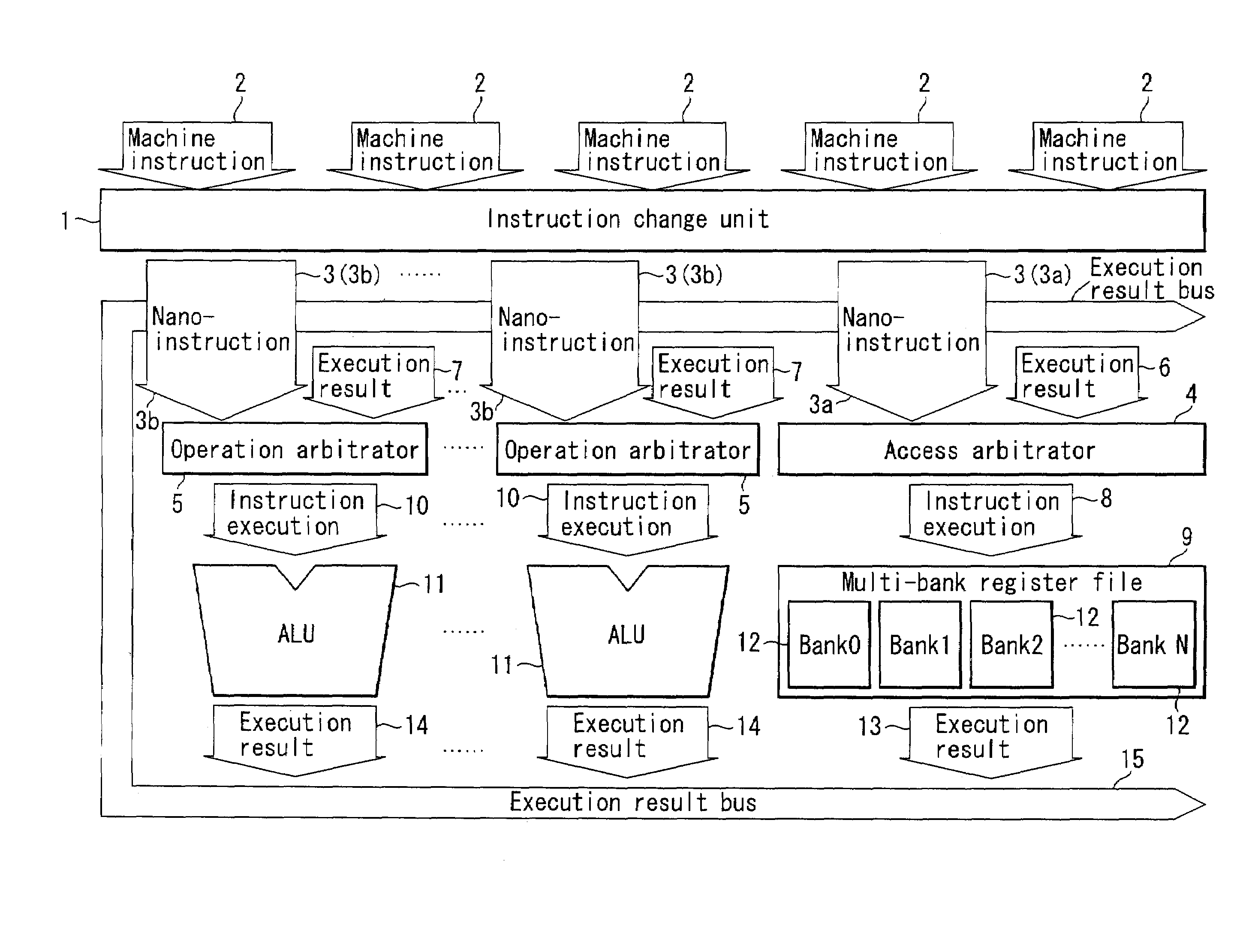
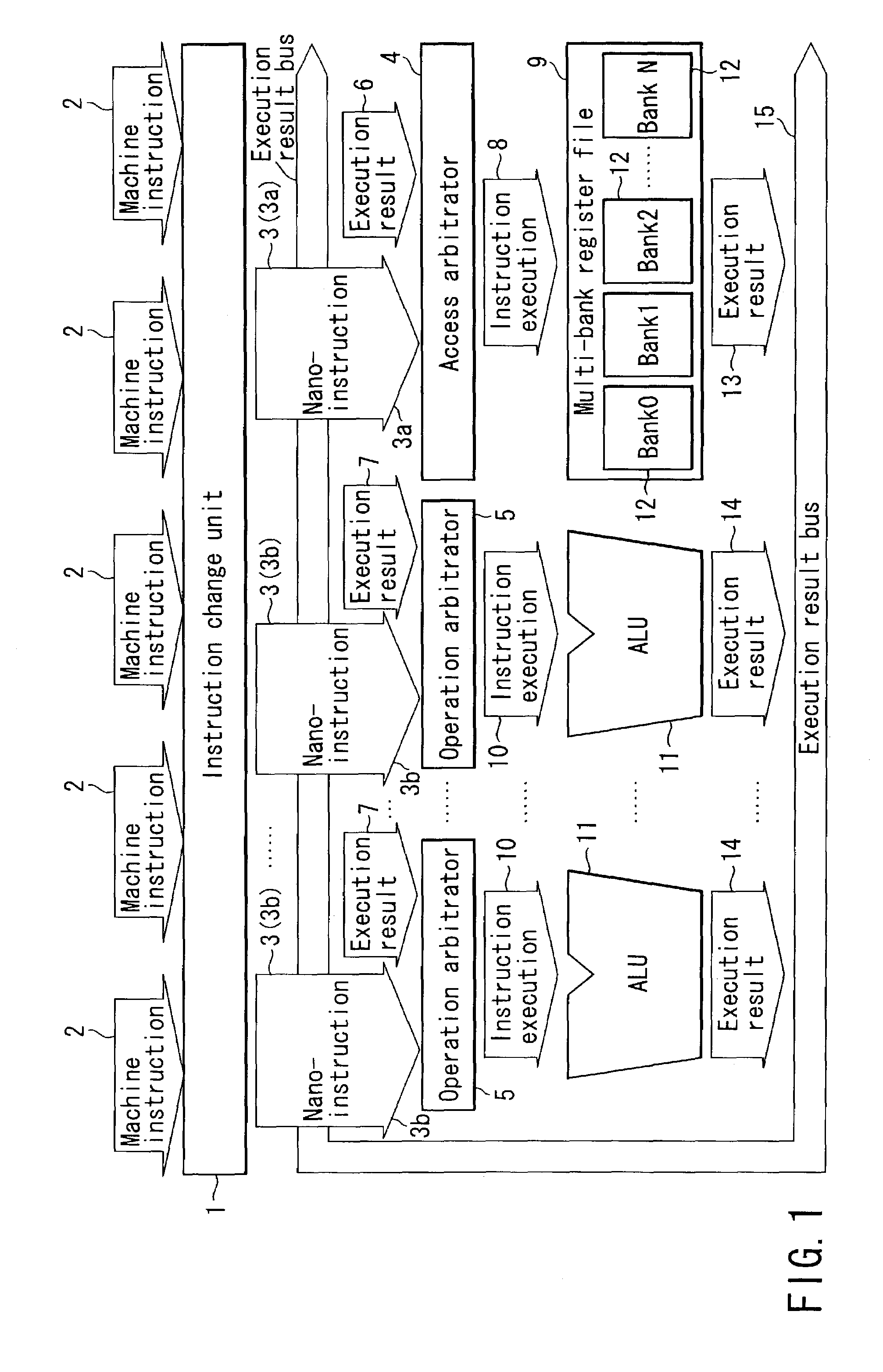
[0067]In the parallel processor of the first embodiment with the above arrangement, the instruction change unit 1 splits each externally input machine instruction 2 into a plurality of nano-instructions 3 (3a, 3b) each of which includes at least one of an access instruction 3a and operation instruction 3b, and allows instruction execution of nano-instructions 3 (3a, 3b) at their own best timings.

[0068]As shown in FIG. 6A, an access instruction 3a to the multi-bank register file 9 and an operation instruction 3b to the operation unit 11 have an identical function level. As a result, the execution timings of a machine instruction 2 which has no access instruction 3a to the register and a machine instruction 2 which can acquire operands only by forwarding can be set earlier, thus increasing the processing speed of the parallel processor.

[0069]Note that FIG. 6B shows the execution sequence of a machine instruction in a conventional parallel processor which does not change a machine inst...

second embodiment

[0076]FIG. 8 is a schematic block diagram showing the arrangement of a parallel processor according to the present invention.

[0077]The parallel processor of the second embodiment can simultaneously execute N instructions 20 which are externally input in one clock cycle.

[0078]An instruction sorter 21 sorts N input instructions 20 into access instructions 22 and operation instructions 23, and respectively outputs them to an access instruction execution unit 24 and an operation instruction execution unit 25. The access instruction execution unit 24 makes accesses designated with bank addresses ABn to a multi-bank register file 26 and register addresses An in banks on the basis of a maximum of N input access instructions 22. The operation instruction execution unit 25 executes a maximum of N input operation instructions 23 with respect to an operation unit (ALU) 27. The access results and operation results are output onto a data bus 28.

[0079]The multi-bank register file 26 has N ports 2...


PUM


Abstract

A parallel processor has a plurality of operation units that execute operation instructions, and a multi-bank register file in which a plurality of banks each having a plurality of registers are formed. Each of machine instructions, which are input simultaneously, is split into a plurality of nano-instructions each of which includes at least one of an access instruction and operation instruction. The output clock cycles of operation instructions with respect to the operation units are arbitrated. Furthermore, the output clock cycles of access instructions to the multi-bank register file are arbitrated so as to prevent access instructions from contending in an identical bank in the multi-bank register file.

Description

CROSS-REFERENCE TO RELATED APPLICATIONS[0001]This application is based upon and claims the benefit of priority from the prior Japanese Patent Application No. 2002-117913, filed Apr. 19, 2002, the entire contents of which are incorporated herein by reference.BACKGROUND OF THE INVENTION[0002]1. Field of the Invention[0003]The present invention relates to a parallel processor which simultaneously executes a plurality of instructions in one clock cycle.[0004]2. Description of the Related Art[0005]For example, a parallel processor represented by a super scalar processor and VLIW (very long instruction word) processor simultaneously executes a plurality of instructions in one clock cycle. In order to supply information (data) used in the plurality of instructions to an operational element and to receive data from the operational element, a register file that temporarily stores a large number of data items is required in the parallel processor.[0006]For example, in order to execute a singl...

Claims


Application Information

Patent Timeline
IPC IPC(8): G06F9/30G06F15/00G06F9/40G06F9/38G06F9/318G06F9/34
CPCG06F9/3012G06F9/3885G06F9/3836G06F9/3017
Inventor HIRONAKA, TETSUOJUERGEN, MATTAUSCH HANSHIRAMATSU, TAKESHI
Owner SEMICON TECH ACADEMIC RES CENT
Why Eureka
Try Eureka