Method and apparatus for testing embedded memory on devices with multiple processor cores

a technology of embedded memory and processor core, which is applied in the direction of detecting faulty computer hardware, error detection/correction, instruments, etc., can solve the problems of reducing the time required to off-load a map of memory failures, reducing the time required for memory test, and easy to be easily damaged by particles

Active Publication Date: 2006-12-26
TEXAS INSTR INC
View PDF18 Cites 31 Cited by
  • Summary
  • Abstract
  • Description
  • Claims
  • Application Information

AI Technical Summary

Benefits of technology

[0006]Disclosed herein is a method and apparatus for testing embedded memory arrays in a computer chip having more than one processor core. According to principles known in the art, a built-in processor may be utilized to test an embedded memory array and generate a memory repair solution for that memory array. The disclosed method and apparatus enables multiple embedded memory arrays associated with multiple processor cores to be simultaneously tested on a single computer chip. According to one aspect, the disclosed method and apparatus identifies certain rows and columns within the embedded memory array that need to be disabled and also identifies certain redundant rows and columns in the embedded memory array to be activated. According to another aspect, the disclosed method and apparatus generates a map indicating where each of the memory failures occurs in an embedded memory array. If the testing process determines that the embedded memory array cannot be repaired, then a signal is provided to an external testing device indicating that the embedded memory array is non-repairable. Similarly, if the testing process determines that the failures in the embedded memory array can be repaired, then a signal is provided to an external testing apparatus indicating that the embedded memory array is repairable. Lastly, if no failures are found in an embedded memory array, then a signal is provided to an external testing apparatus indicating that the embedded memory array contains no failures. Based upon these status signals, the external testing device can determine which set of data (i.e., repair data and / or failure map data) to off-load from the embedded memory device and which sets of data to disregard, thereby reducing the memory test time for a device. Another aspect of the disclosed method and apparatus is a data flow control unit that controls the flow of input and output data to each of the embedded memory arrays. This device broadcasts the test program to each of the embedded memory arrays at the same time thereby enabling the simultaneous testing of multiple embedded memory arrays. Yet another aspect of the disclosed method and apparatus is a shorthand notation for indicating where memory failures occur within an embedded memory array. By utilizing this shorthand notation, the time required to off-load a map of the memory failures is greatly reduced. These features, as well as many other features and aspects, are described in further detail in the following detailed description.

Problems solved by technology

Because memory devices utilize very small features, one problem associated with the fabrication of these devices is that they are easily subject to damage from particles, lithographic misalignment, scratches, and other fabrication errors.
If it is determined that the memory array cannot be repaired, then the device is scrapped before costly and time-consuming back-end processes (i.e. packaging) are performed.
Although this process works well for a single core (i.e. processor) chip, its implementation on a multiple-core chip becomes much more complicated.

Method used


Image

  • Method and apparatus for testing embedded memory on devices with multiple processor cores
  • Method and apparatus for testing embedded memory on devices with multiple processor cores
  • Method and apparatus for testing embedded memory on devices with multiple processor cores

Examples


Embodiment Construction

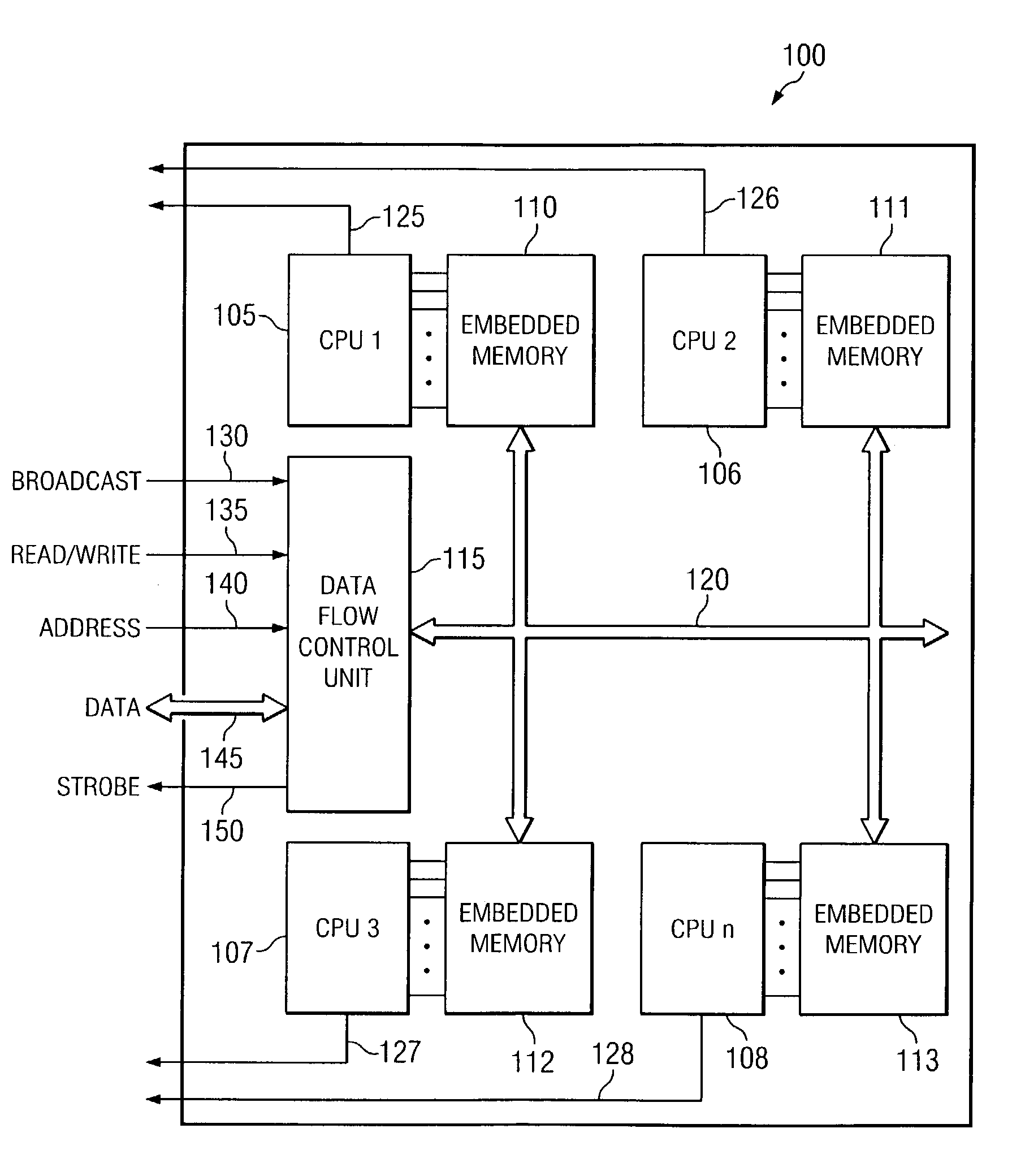
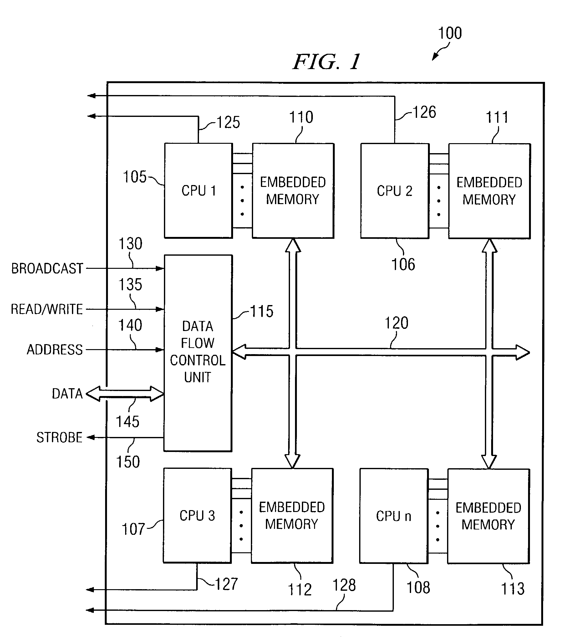
[0012]A block diagram depicting a computer chip suitable for use with the disclosed method and apparatus is depicted in FIG. 1. In FIG. 1, the computer chip 100 is comprised of four separate processors 105, 106, 107, 108. Each of these processors is associated with an embedded memory cache 110, 111, 112, 113. Also depicted in FIG. 1 is a data flow control unit 115. The data flow control unit 115 receives information from an external tester and provides that information to each of the embedded memory caches 110, 111, 112, 113. To accomplish this, the data flow control unit 115 is connected to each of the embedded memory caches 110, 111, 112, 113 through a data bus 120. Also depicted in FIG. 1 are four processor status indicators 125, 126, 127, 128. According to one embodiment, each of these processor status indicators comprises a two-bit signal line that indicates the pass, fail, or repair status of an embedded memory cache associated with each corresponding processor. The processor ...


PUM


Abstract

The disclosed method and apparatus enables the testing of multiple embedded memory arrays associated with multiple processor cores on a single computer chip. According to one aspect, the disclosed method and apparatus identifies certain rows and columns within each of the embedded memory arrays that need to be disabled and also identifies certain redundant rows and columns in the embedded memory array to be activated. According to another aspect, the disclosed method and apparatus generates a map indicating where each of the memory failures occurs in each embedded memory array. If the testing process determines that the embedded memory array cannot be repaired, then a signal is provided directly to an external testing device indicating that the embedded memory array is non-repairable. Similarly, if the testing process determines that the failures in the embedded memory array can be repaired, then a signal is provided directly to an external testing apparatus indicating that the embedded memory array is repairable. Lastly, if no failures are found in an embedded memory array, then a signal is provided to an external testing apparatus indicating that the embedded memory array contains no failures. Based upon these status signals, the external testing device can determine which set of data (i.e., repair data and / or failure map data) to off-load from each embedded memory array and which sets of data to disregard, thereby reducing the memory test time for a device. Another aspect of the disclosed method and apparatus is a data flow control unit that controls the flow of input and output data to each of the embedded memory arrays. This device broadcasts the test program to each of the embedded memory arrays at the same time thereby enabling the simultaneous testing of multiple embedded memory arrays. Yet another aspect of the disclosed method and apparatus is a shorthand notation for indicating where memory failures occur within an embedded memory array.

Description

CROSS REFERENCE TO RELATED APPLICATIONS[0001]This patent application claims priority to provisional patent application No. 60 / 443,946 entitled “processor-Based Test Methodology for Embedded Memory on Devices with Multiple processor Cores,” which has a filing date of Jan. 31, 2003 and is hereby incorporated by reference into the specification of this application.BACKGROUND[0002]The integrated circuit industry is under continuous pressure to reduce the size of the components on integrated circuits and to increase the number of devices that can be integrated onto a single chip. These market forces have been associated with what is known in the industry as Moore's Law. Moore's Law suggests that the number of transistors that can be fabricated on an integrated circuit doubles approximately every 18 to 20 months. Although Moore's Law is based upon purely empirical and historical data, it has been proven to be a reliable indicator of trends in the integrated circuit industry.[0003]These ma...

Claims


Application Information

Patent Timeline
IPC IPC(8): G06F11/00G01R31/28G06F11/22G06F12/16G06F15/78G11C29/08G11C29/44H01L27/10
CPCG11C29/08
Inventor JARBOE, JR., JAMES MICHAELWRIGHT, NATHAN WEYERSCHUTT, NICHOLAS HENRYHO, VAN
Owner TEXAS INSTR INC
Why Eureka
Try Eureka