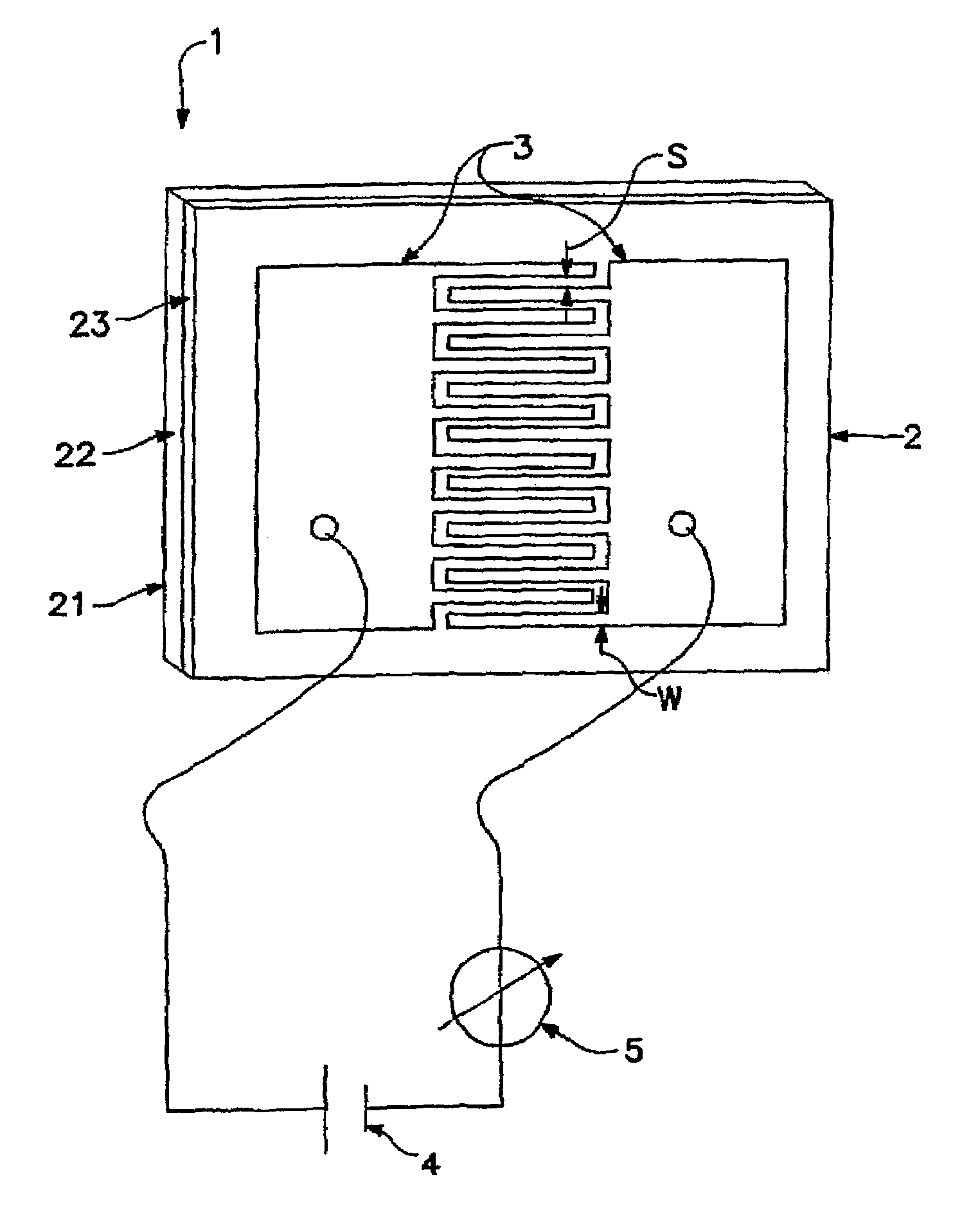
MgZnO based UV detectors
a technology of ultraviolet detection and detector, applied in the field of optoelectronic applications, can solve the problems of lateral geometry of the conductor device, and the inability to accurately detect the material of the detector
- Summary
- Abstract
- Description
- Claims
- Application Information
AI Technical Summary
Benefits of technology
Problems solved by technology
Method used
Image

Examples
example 1
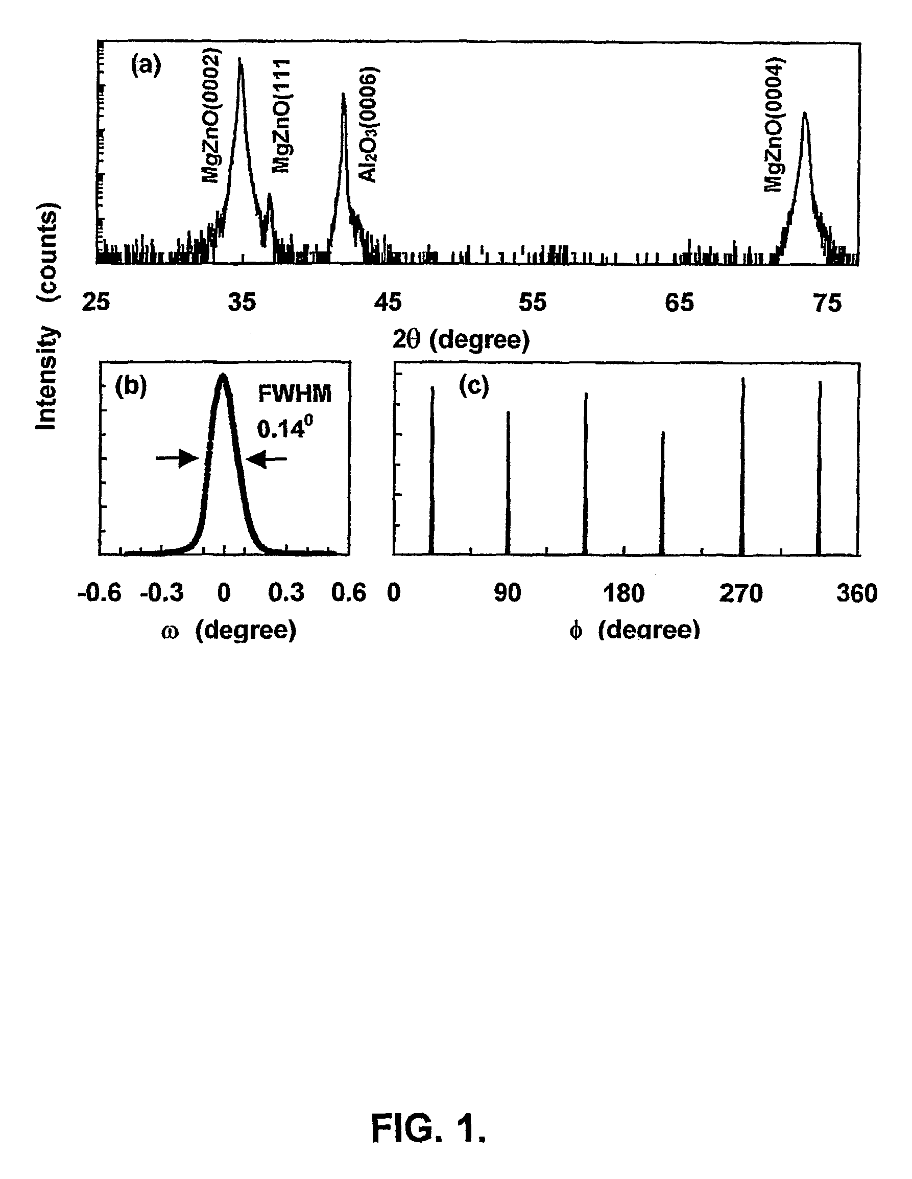
[0052]FIG. 1 is an XRD Θ-2Θ scan of (a) c-MgZnO / Si(100), (b)c-MgZnO / STO / SrO / Si (100), (c) c-MgZnO / STO / TiN / Si(100) (d) c-MgZnO / BTO / YSZ / Si(100). The c-MgZnO films were grown at 600° C. with oxygen partial pressure of 1×10⁻⁶ torr. The film thickness is 2000–5000 Å. The plot is in semi-logarithm scale. FIG. 1 is the XRD Θ-2Θplot of c-MgZnO films grown on Si(100) with various buffer layers. The result of c-MgZnO films grown directly on Si(100) without any buffer is also provided as a reference. As can be seen from FIG. 1(a) that without a buffer layer, only a broad MgZnO(111) peak appears at 2Θ=36.8° (FIG. 1-a). The intensity of this peak is more than four orders of magnitudes lower than that of Si(400), indicating that the film is essentially amorphous. Due to the large lattice mismatch, the epitaxial growth of c-MgZnO on Si(100) can only be obtained when proper buffers are applied. FIGS. 1(b)(c)(d) show that the crystalline quality of the c-MgZnO films was improved significantly when a...
example 2
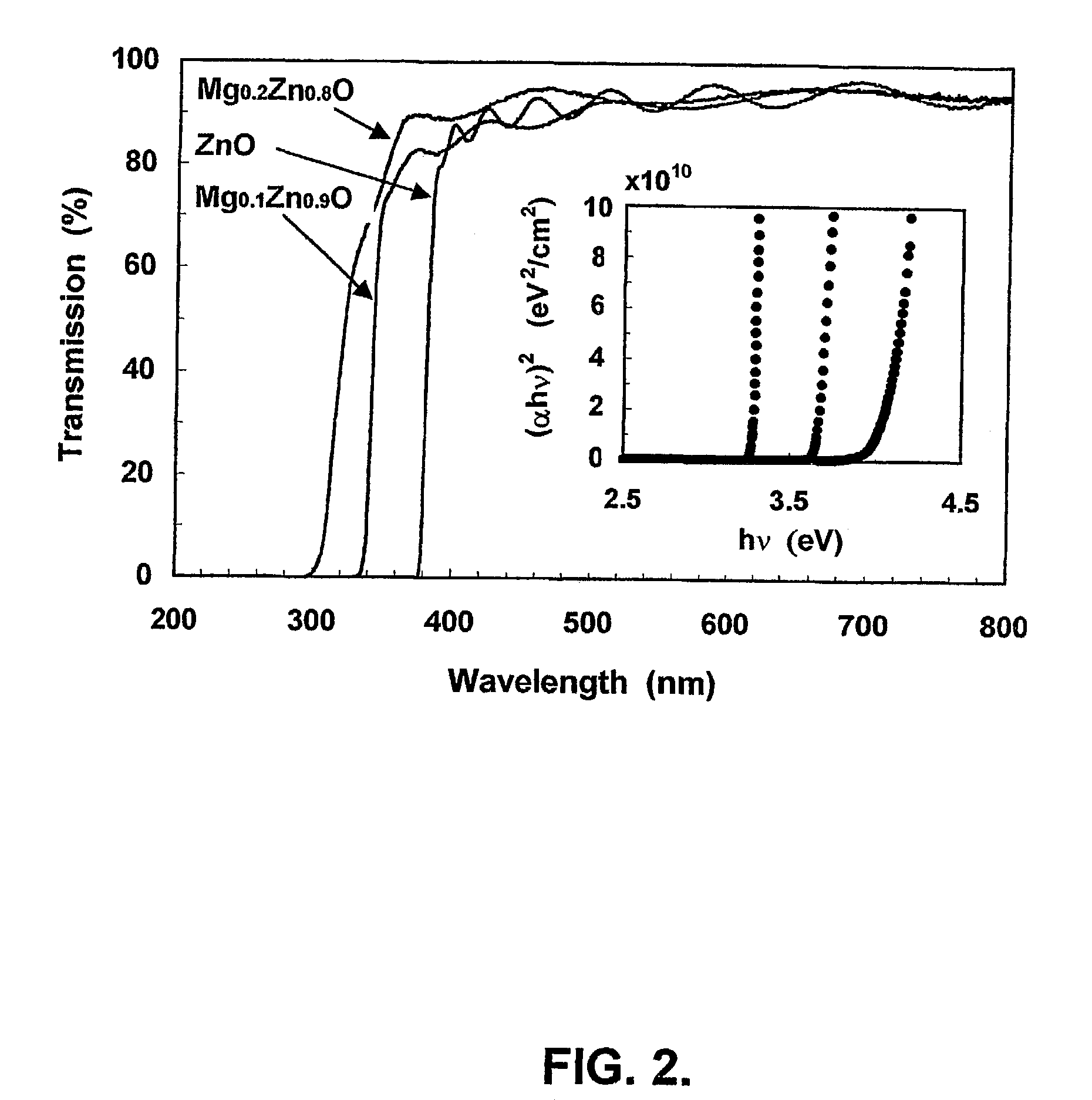
[0053]FIG. 2 is an XRD Φ scan of c-MgZnO / STO / SrO / Si (b) c-MgZnO / BTO / YSZ / Si. The in-plane alignment of c-MgZnO, buffer layer and Si is indicated by the position of diffraction peaks. The epitaxial growth of c-MgZnO on Si (100) is further confirmed by the XRD-scan Φ shown in FIG. 2. For c-MgZnO grown on all three sets of buffer layers, i.e. STO / SrO, STO / TiN, BTO / YSZ, the Φ scans show 4-fold azimuth symmetry, indicating the cubic crystal structure of c-MgZnO. The average full width at half maximum (FWHM) of c-MgZnO is 0.5° for c-MgZnO with STO / SrO buffer, 0.7° for c-MgZnO with BTO / YSZ buffer, compared with the 0.4° of Si(100). The line width of c-MgZnO grown on STO / TiN / Si(100) is slightly larger (˜1°) due to the poor interface between TiN and Si.
[0054]Except for STO / SrO, the maximum Φ-scan diffraction of c-MgZnO is at the same angle as that of buffer layer and Si substrate, indicating the in-plane alignment is c-MgZnO [100] / / buffer [100] / / Si[100]. For STO / SrO buffer, however, the four ...
example 3
[0056]FIG. 3 depicts full width at half maximum (FWHM) of c-MgZnO(200) rocking as curves functions of (a) PLD deposition temperature and (b) oxygen pressure. The c-MgZnO films are grown on STO / SrO / Si(100) (*), BTO / YSZ / Si(100) (**) and STO / TiN / Si(100) ( ). To find the optimal PLD growth conditions, the XRD line widths of c-MgZnO grown at different conditions were measured, which serve as an indicator of c-MgZnO crystalline quality. Shown in FIG. 3 is the FWHM of co-rocking curves of c-MgZnO as functions of substrate temperature and oxygen partial pressure. As shown in FIG. 3(a), for substrate temperatures from 30° C., to 600° C., the FWHM of ω-rocking curves decrease sharply from 2.5° to 0.23°, indicating the significant improvement of crystalline quality. Above 600° C., the narrowing of a XRD line width is not significant. At 800° C., a broadening of XRD rocking curve to 0.28° was observed, which may be caused by the change of chamber base pressure due to the degassing of the substr...
PUM
 Abstract
Description
Claims
Application Information
 - R&D
- Intellectual Property
- Life Sciences
- Materials
- Tech Scout
- Unparalleled Data Quality
- Higher Quality Content
- 60% Fewer Hallucinations
Browse by: Latest US Patents, China's latest patents, Technical Efficacy Thesaurus, Application Domain, Technology Topic, Popular Technical Reports.
© 2025 PatSnap. All rights reserved.Legal|Privacy policy|Modern Slavery Act Transparency Statement|Sitemap|About US| Contact US: help@patsnap.com