Memory device for burst or pipelined operation with mode selection circuitry

a memory device and mode selection technology, applied in the field of memory device architectures, can solve the problems of data the price per bit of these memory devices is continually declining, and the data may still be valid for a few nanoseconds, so as to achieve fast data access, high speed data access, and high speed

Inactive Publication Date: 2006-10-17
MICRON TECH INC
View PDF71 Cites 1 Cited by
  • Summary
  • Abstract
  • Description
  • Claims
  • Application Information

AI Technical Summary

Benefits of technology

[0010]An integrated circuit memory device with a standard DRAM pinout is designed for high speed data access and for compatibility with existing memory systems. A high speed burst mode of operation is provided where multiple sequential accesses occur following a single column address, and read data is output relative to the / CAS control signal. In the burst mode of operation the address is incremented internal to the device eliminating the need for external address lines to switch at high frequencies. Read / Write commands are issued once per burst access eliminating the need to toggle the Read / Write control line at high speeds. Only one control line per memory chip ( / CAS) must toggle at the operating frequency in order to clock the internal address counter and the data input / output latches. The load on each / CAS is typically less than the load on the other control signals ( / RAS, / WE and / OE) since each / CAS typically controls only a byte width of the data bus. Internal circuitry of the memory device is largely compatible with existing Extended Data Out (EDO) DRAMs. This similarity allows the two part types to be manufactured on one die with a limited amount of additional circuitry. The ability to switch between a standard non-burst mode and a high speed burst mode allows the device to be used to replace standard devices, and eliminates the need to switch to more complex high speed memory devices. Internal address generation provides for faster data access times than is possible with either fast page mode or EDO DRAMs. This high speed operation eliminates the need to interleave memory devices in order to attain a high data throughput. In contrast to the 50 megahertz interleaved memory system described above, the output data from this device will be valid for approximately 15 nanoseconds significantly easing the design of circuitry required to latch the data from the memory. The device is compatible with existing memory module pinouts including Single In-Line Memory Module (SIMM), Multi-Chip Module (MCM) and Dual In-Line Memory Module (DIMM) designs. This combination of features allows for significant system performance improvements with a minimum of design alterations.
[0015]Additionally, the present invention facilitates an integrated circuit chip with pinouts identical to those of prior asynchronous memories. Alternatively, the present invention provides a new pinout which includes a pin which may be assigned to accept an external mode select control signal. The present invention also provides a memory module having external mode select control.

Problems solved by technology

Except for their high volume production, the state of the art manufacturing requirements of these devices would cause them to be exorbitantly priced.
Yet, due to efficiencies associated with high volume production, the price per bit of these memory devices is continually declining.
This high speed circuitry has allowed for faster page mode cycle times. A problem exists in the reading of a DRAM when the device is operated with minimum fast page mode cycle times. / CAS may be low for as little as 15 nanoseconds, and the data access time from / CAS to valid output data (tCAC) may be up to 15 nanoseconds; therefore, in a worst case scenario there is no time to latch the output data external to the memory device.
For devices that operate faster than the specifications require, the data may still only be valid for a few nanoseconds.
On a heavily loaded microprocessor memory bus, trying to latch an asynchronous signal that is valid for only a few nanoseconds is very difficult.
Even providing a new address every 35 nanoseconds requires large address drivers which create significant amounts of electrical noise within the system.
Methods to shorten memory access cycles tend to require additional circuitry, additional control pins and nonstandard device pinouts.
The addition of several control pins has required a deviation in device pinout from standard DRAMs which further complicates design efforts to utilize these new devices.
Significant amounts of additional circuitry are required in the SDRAM devices which in turn result in higher device manufacturing costs.
Additionally, existing computer system memory architectures are designed such that control and address signals may not be able to switch at the frequencies required to operate the new memory device at high speed due to large capacity loads on the signal lines.
These lines inherently have high capacitive loads as a result of the number of device inputs driven by them.
SIMM devices also typically ground the output enable ( / OE) pin making / OE a less attractive candidate for providing extended functionality to the memory devices.
There is a great degree of resistance to any proposed deviations from the standard SIMM design due to the vast number of computers which use SIMMs.
Industry's resistance to radical deviations from the standard, and the inability of current systems to accommodate the new memory devices will delay their widespread acceptance.
Therefore only limited quantities of devices with radically different architectures will be manufactured initially.
However, prior asynchronous DRAMs did not have both burst and pipelined modes of operation.
Thus, such prior asynchronous DRAMs did not support applications requiring both modes of operation.

Method used


Image

  • Memory device for burst or pipelined operation with mode selection circuitry
  • Memory device for burst or pipelined operation with mode selection circuitry
  • Memory device for burst or pipelined operation with mode selection circuitry

Examples


Embodiment Construction

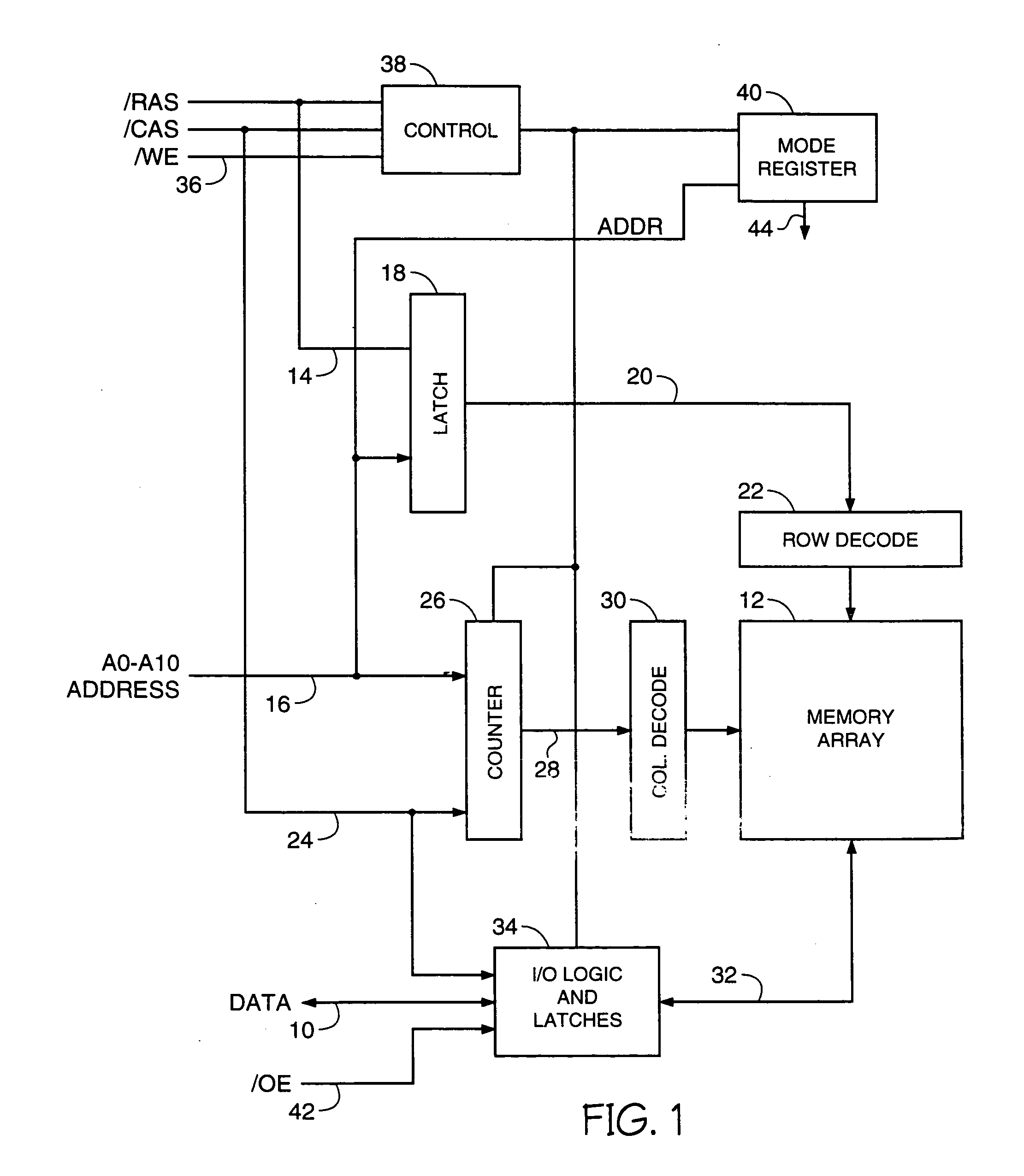
[0037]FIG. 1 is a schematic representation of a sixteen megabit device designed in accordance with the present invention. The device is organized as a 2 Meg×8 burst EDO DRAM having an eight bit data input / output path 10 providing data storage for U.S. Pat. No. 2,097,152 bytes of information in the memory array 12. The device of FIG. 1 has an industry standard pinout for eight bit wide EDO DRAMs. An active-low row address strobe ( / RAS) signal 14 is used to latch a first portion of a multiplexed memory address, from address inputs A0 through A1016, in latch 18. The latched row address 20 is decoded in row decoder 22. The decoded row address is used to select a row of the memory array 12. A column address strobe ( / CAS) signal 24 is used to latch a second portion of a memory address from address inputs 16 into column address counter 26. The latched column address 28 is decoded in column address decoder 30. The decoded column address is used to select a column of the memory array 12.

[003...


PUM


Abstract

An integrated circuit memory device is designed for high speed data access and for compatibility with existing memory systems. An address strobe signal is used to latch a first address. During a burst access cycle the address is incremented internal to the device with additional address strobe transitions. A new memory address is only required at the beginning of each burst access. Read / Write commands are issued once per burst access eliminating the need to toggle the Read / Write control line at the device cycle frequency. Transitions of the Read / Write control line during a burst access will terminate the burst access, reset the burst length counter and initialize the device for another burst access. The device is compatible with existing Extended Data Out DRAM device pinouts, Fast Page Mode and Extended Data Out Single In-Line Memory Module pinouts, and other memory circuit designs. Additionally, a DRAM is provided having both pipelined and burst Extended Data Out modes of operation and the ability to switch between them.

Description

[0001]This application is a divisional of application Ser. No. 08 / 650,719, filed May 20, 1996, which is a Continuation-In-Part of application Ser. No. 08 / 584,600, filed Jan. 1, 1996, now U.S. Pat. No. 5,966,724.CROSS-REFERENCE TO RELATED APPLICATION[0002]The below listed applications, as indicated by serial number and filing date, are all assigned to the assignee of the instant application and were or are co-pending with and related to the instant application: Ser. No. 08 / 370,761, filed Dec. 23, 1994 (now U.S. Pat. No. 5,526,320, issued Jun. 11, 1996); Ser. No. 08 / 386,894, filed Feb. 10, 1995 (now U.S. Pat. No. 5,610,864, issued Mar. 11, 1997); Ser. No. 08 / 386,563, filed Feb. 10, 1995 (now U.S. Pat. No. 5,652,724, issued Jul. 29, 1997); Ser. No. 08 / 457,650, filed Jun. 1, 1995 (pending); Ser. No. 08 / 457,651, filed Jun. 1, 1995 (now U.S. Pat. No. 5,675,549, issued Oct. 7, 1997); Ser. No. 08 / 497,354, filed Jun. 30, 1995 (now U.S. Pat. No. 5,598,376, issued Jan. 28, 1997); Ser. No. 08 / 5...

Claims


Application Information

Patent Timeline
Patent Type & Authority Patents(United States)
IPC IPC(8): G06F12/00G11C7/00G11C7/10
CPCG11C7/1015G11C7/1024G11C7/1027G11C7/1039G11C7/1045G11C7/20
Inventor MAILLOUX, JEFFREY S.RYAN, KEVIN J.MERRITT, TODD A.WILLIAMS, BRETT L.
Owner MICRON TECH INC
Why Eureka
Try Eureka