High-speed electro-absorption modulator with low drive voltage

a high-speed, drive-voltage technology, applied in the field of electro-absorption modulators, can solve the problems of limiting the performance of traveling-wave electrodes, too low impedances of components, and large insertion loss, so as to increase the confinement factor of light and reduce the insertion loss of ligh

Inactive Publication Date: 2006-09-05
NAT CENT UNIV
View PDF6 Cites 9 Cited by
  • Summary
  • Abstract
  • Description
  • Claims
  • Application Information

AI Technical Summary

Benefits of technology

[0004]Therefore, the main purposes of the present invention is to release the trade-off between the drive voltage and the speed, to increase the confinement factor of the light in the un-doped layer, and to reduce the insertion loss of the light caused by the free-carrier absorption in the doped layer.
[0005]To achieve the above purposes, the present invention is a high-speed EAM with low drive voltage, comprising a p-i-n-i-n epitaxy layer formed on a semiconductor substrate 2. The p-i-n-i-n epitaxy layer 1 comprises a p-doped layer, a first intrinsic layer (i-layer), a first n-doped layer (n-layer), a second i-layer and a second n-layer, which are grown as epitaxy layers to obtain the EAM. The epitaxy structure of the EAM according to the present invention is p-i(MQW)-n+-i(collector)-n. Because the first n-layer is inserted into the un-doped depletion layer to be an electric-field confining layer so that most of the electric field is concentrated in the first i-layer (MQW) to avoid the increase of the drive voltage while the thickness of the second i-layer (collector) is increased. Besides, the thickness of the un-doped layer is greatly increased. Accordingly, the trade-off between the drive voltage and the speed can be released, the confinement factor of the light in the un-doped layers can be increased, and the insertion loss of the light caused by the free-carrier absorption in the doped regions can be reduced.

Problems solved by technology

The EAM of the prior art has a big insertion loss and the impedances of the components are too low, which limits its performance with traveling-wave electrode structure.
Yet, the biggest problem of the p-i-n epitaxy structure is as follows: In order to reduce the operation voltage, the thickness of the i-layer can not be thick; but a thin i-layer has a quite big device capacitance so that the performance of the component becomes worse.
However, a thick intrinsic layer and a small device size imply a high operation voltage and a serious optical coupling / insertion loss, respectively.

Method used


Image

  • High-speed electro-absorption modulator with low drive voltage
  • High-speed electro-absorption modulator with low drive voltage
  • High-speed electro-absorption modulator with low drive voltage

Examples


Embodiment Construction

[0015]The following descriptions of the preferred embodiments are provided to understand the features and the structures of the present invention.

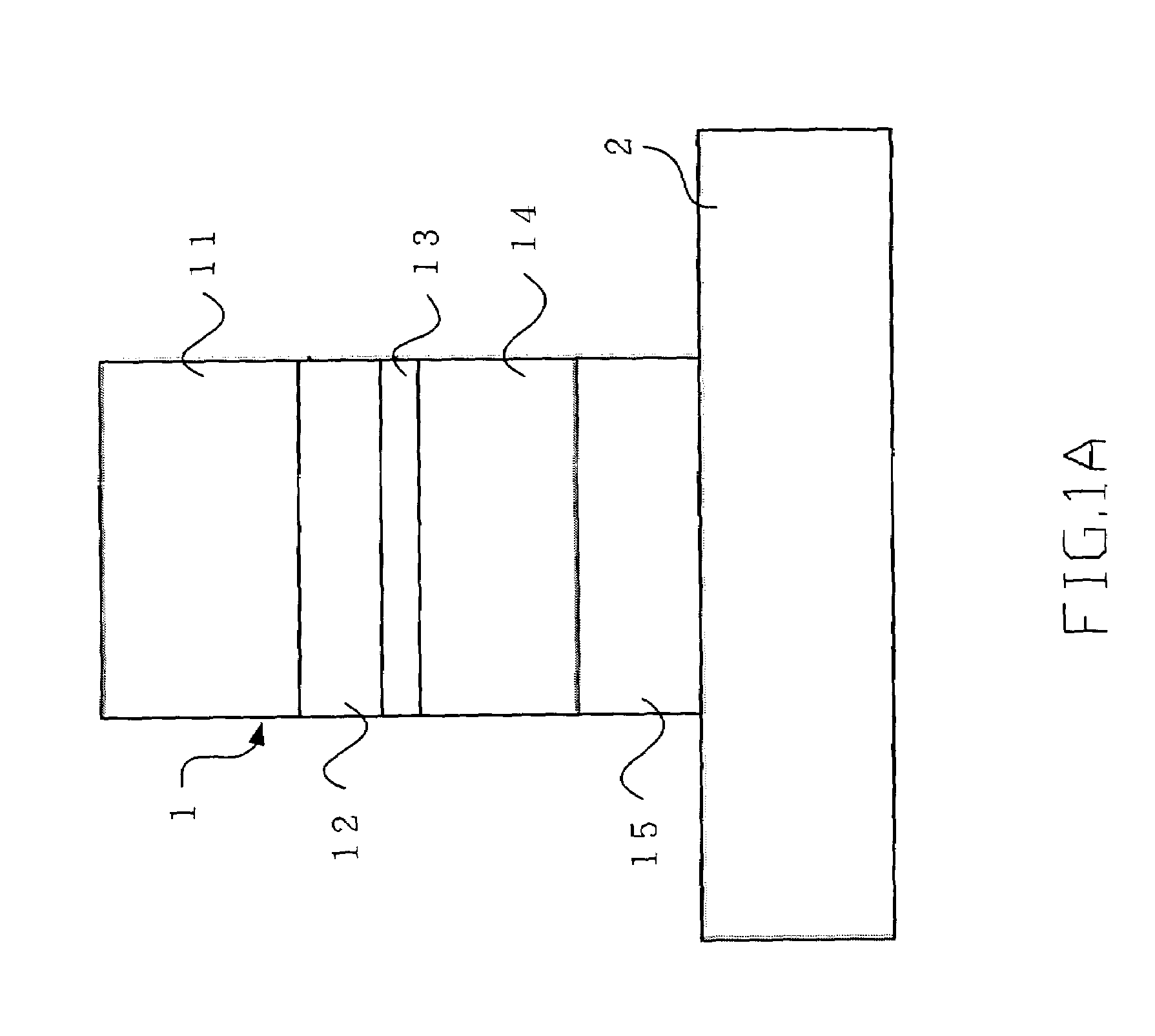
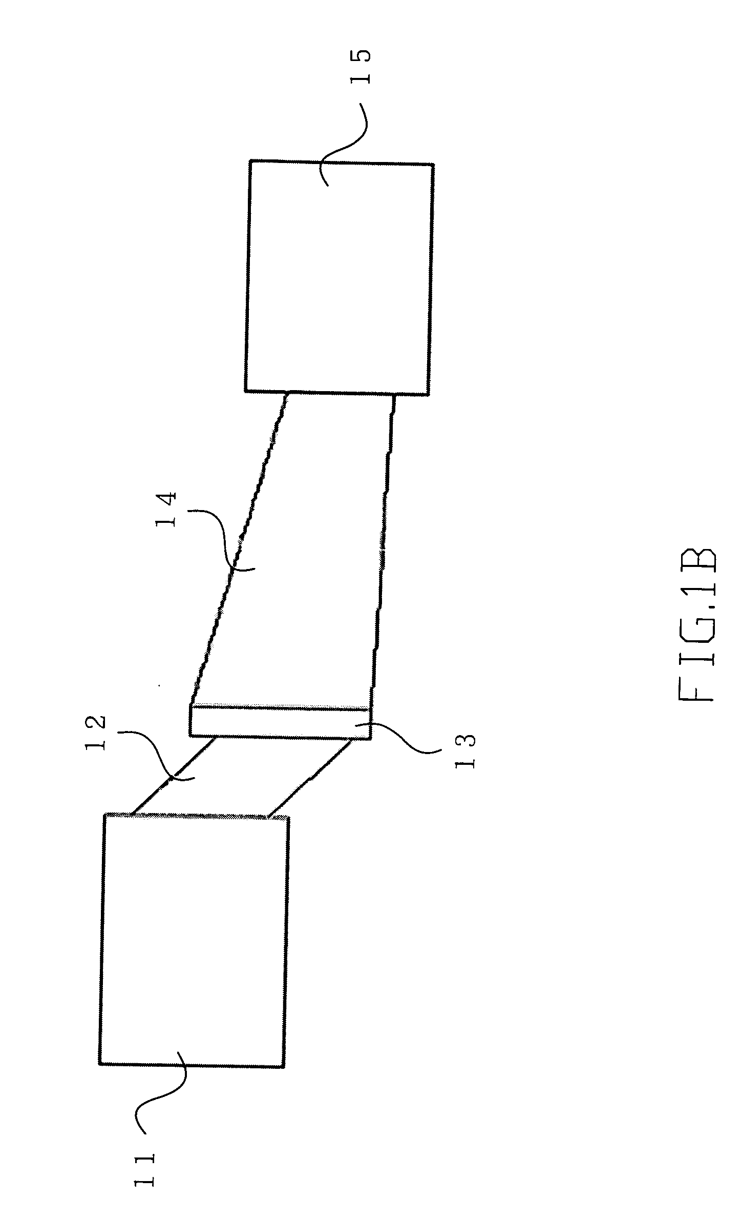
[0016]Please refer to FIG. 1A and FIG. 1B, which, according to the present invention, are views showing an epitaxy structure of an EAM and the EAM itself. As shown in the figures, The present invention is an EAM, comprising a p-i-n-i-n epitaxy layer 1 (formed by doping GaAs, InP and GaN; or by doping AIN, Si and GaSb) formed on a semiconductor substrate 2. The p-i-n-i-n epitaxy layer 1 comprises a second intrinsic layer 14 (i-layer) formed on a second n-doped layer 15 (n-layer); a first n-layer 13 formed on the second i-layer 14; a first i-layer 12 formed on the first n-layer 13; and a p-doped layer 11 (p-layer) formed on the first i-layer 12. Its structure is formed by a semiconductor of any compound (such as GaAs, InP or GaN) or any column element together with a semiconductor of its alloy (such as a compound semiconductor of AlGaN InGaN...


PUM

PropertyMeasurementUnit
wavelength operationaaaaaaaaaa
wavelengthaaaaaaaaaa
widthaaaaaaaaaa

Abstract

The present invention is an electro-absorption modulator with a p-i-n-i-n epitaxy layer whose structure is p-i(MQW)-n+-i(collector)-n to release the trade-off between the operation voltage and the speed, to increase the confinement factor of the light in the un-doped layers, and to reduce the insertion loss caused by the free-carrier absorption in the doped layers, wherein MQW stands for Multiple-Quantum Well.

Description

FIELD OF THE INVENTION[0001]The present invention relates to an electro-absorption modulator; more particularly, relates to a p-i-n-i-n epitaxy layer with an epitaxy structure of p-i(MQW)-n+-i(collector)-n which is grown on a semiconductor substrate and can be applied to an optical modulator, wherein MQW stands for Multiple-Quantum Well.DESCRIPTION OF THE RELATED ART[0002]In modern high-speed optical communication system, an optical modulator with a speed over 10 Gbps (bits per second) is a very critical part. The optical modulators used today are mainly divided into two kinds: some are Electro-Absorption Modulators (EAM) and the others are Electro-Optics Modulators (EOM). The EAM of the prior art has a big insertion loss and the impedances of the components are too low, which limits its performance with traveling-wave electrode structure.[0003]Please refer to FIG. 5, which is a view showing a structure of an epitaxy of an EAM according to the prior art. As shown in the figure, the ...

Claims


Application Information

Patent Timeline
Patent Type & Authority Patents(United States)
IPC IPC(8): G02F1/03
CPCB82Y20/00G02F1/017G02F1/01725G02F1/01708
Inventor SHI, JIN-WEIHSIEH, CHEN-AN
Owner NAT CENT UNIV
Why Eureka
Try Eureka