Semiconductor memory having two charge storage sections
a technology of semiconductor memory and charge storage section, which is applied in the field of semiconductor memory, can solve the problems of obstructing further miniaturization of the device, difficulty in 2 bit operation, etc., and achieves the effect of easy miniaturization
- Summary
- Abstract
- Description
- Claims
- Application Information
AI Technical Summary
Benefits of technology
Problems solved by technology
Method used
Image

Examples
embodiment 1
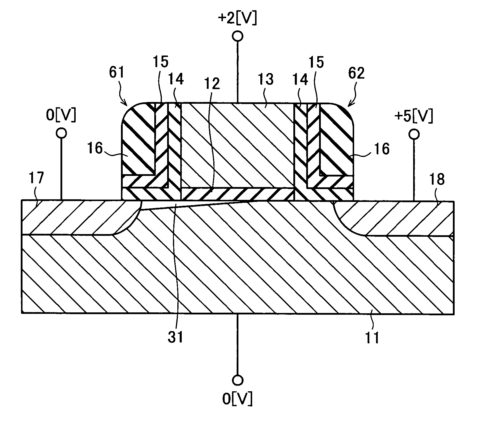
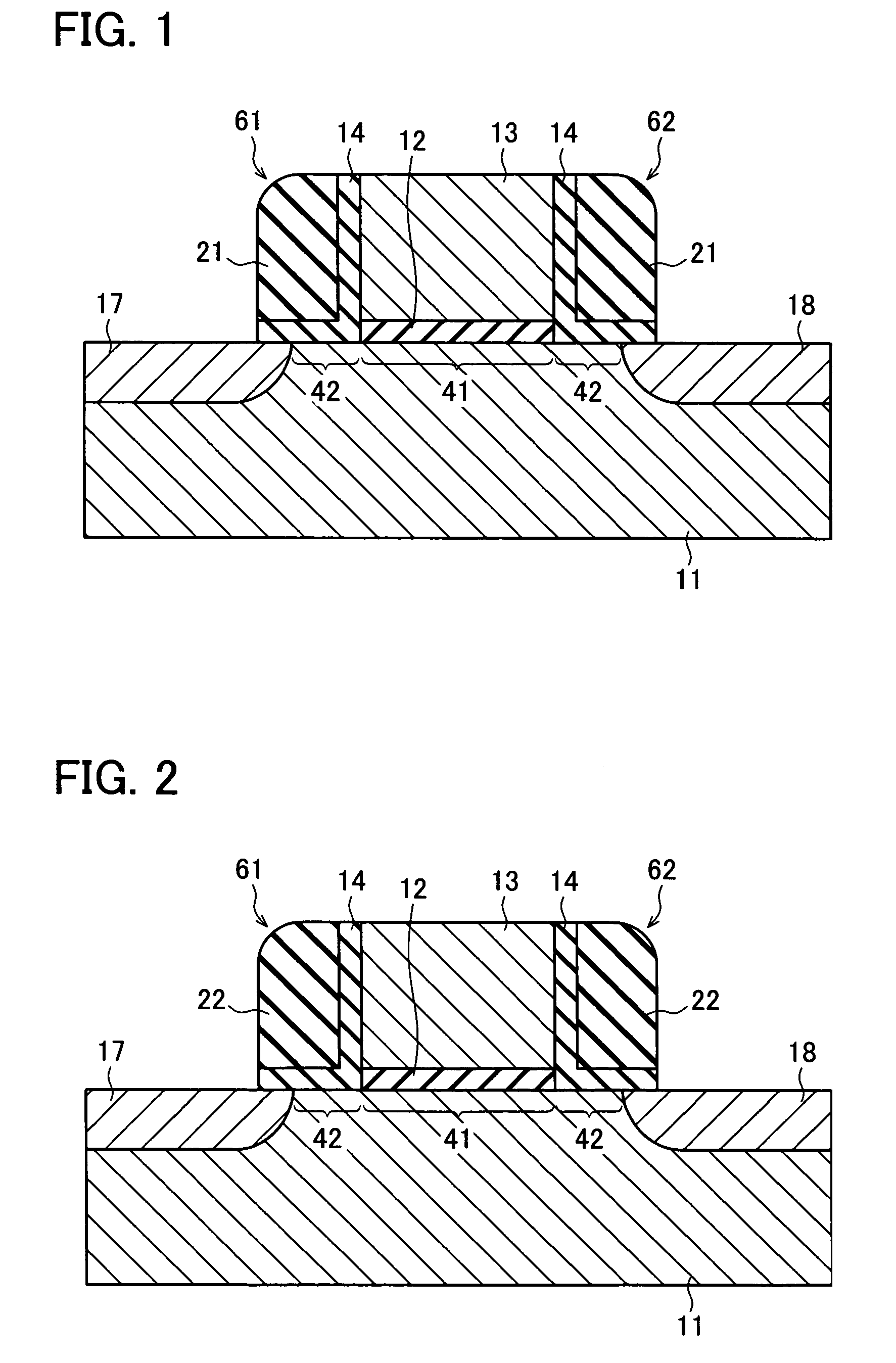
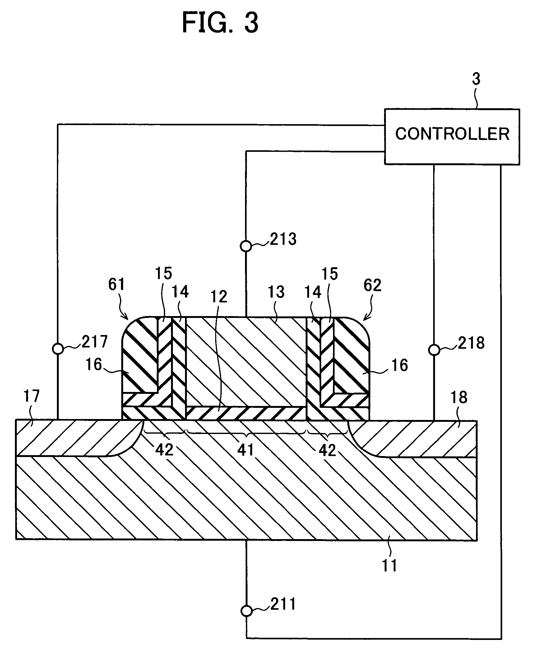
[0083]Referring to FIG. 1 to FIG. 3, the structure of a memory element which is a semiconductor memory in accordance with the present embodiment will be described. FIG. 1 to FIG. 3 are schematic cross-sectional views of the memory element and show different side wall spacer shapes in the charge storage section structure.
[0084]A memory element constituting the semiconductor memory in accordance with the present embodiment is an involatile memory cell capable of storing 2 bits of data. As shown in FIG. 1 to FIG. 3, the semiconductor memory includes a gate electrode 13 formed on a semiconductor substrate 11 with an intervening gate insulating film 12. The electrode 13 has substantially the same gate length as ordinary transistors. On the side walls of the gate insulating film 12 and the gate electrode 13, there are provided charge storage sections 61, 62 shaped like side wall spacers. Opposite to the gate electrode 13, the charge storage sections 61, 62 have a first diffusion layer reg...
embodiment 2
[0120]A semiconductor memory in accordance with the embodiment relates to, in the semiconductor memory in accordance with the first embodiment, preferable positional relationship between the charge storage sections and the diffusion layer regions and a preferable structure of the charge storage sections.
[0121]The semiconductor memory in accordance with the embodiment includes, as shown in FIG. 8, charge storage sections 161, 162 which have regions storing electric charge (which may be regions retaining electric charge and a film capable of storing electric charge) and regions preventing charge leaks (which may be a film preventing charge leaks). An example is the ONO structure. Specifically, a film (charge storing film) 142 made of silicon nitride as the first insulator is sandwiched between a film (first insulating film) 141 made of silicon oxides as the second insulator and a film (second insulating film) 143 made of silicon oxides as the third insulator, so as to form the charge ...
embodiment 3
[0136]This embodiment relates to the structure of the charge storing film 142 in the semiconductor memory in accordance with the second embodiment. In accordance with the embodiment, as shown in FIG. 13, the charge storing film 142 in the charge storage section 162 has a substantially uniform thickness and is made up of a first section 181 substantially parallel to the surface of the gate insulating film 114 and a second section 182 substantially parallel to a side face of the gate electrode 117.
[0137]When positive voltage is applied to the gate electrode 117, the lines of electric force in the charge storage section 162 pass through the silicon nitride film 142 twice (the first section 181 and the second section 182) as indicated by an arrow 183. When negative voltage is applied to the gate electrode 117, the direction of the lines of electric force is opposite. Here, the silicon nitride film 142 has a relative permittivity of about 6, and the silicon oxide films 141, 143 have a re...
PUM
 Abstract
Description
Claims
Application Information
 - R&D
- Intellectual Property
- Life Sciences
- Materials
- Tech Scout
- Unparalleled Data Quality
- Higher Quality Content
- 60% Fewer Hallucinations
Browse by: Latest US Patents, China's latest patents, Technical Efficacy Thesaurus, Application Domain, Technology Topic, Popular Technical Reports.
© 2025 PatSnap. All rights reserved.Legal|Privacy policy|Modern Slavery Act Transparency Statement|Sitemap|About US| Contact US: help@patsnap.com