
Method for the manufacture of a printed circuit and planar antenna manufactured with this printed circuit

Inactive Publication Date: 2006-06-13
MICROCONNECTIONS
View PDF11 Cites 18 Cited by
  • Summary
  • Abstract
  • Description
  • Claims
  • Application Information

AI Technical Summary

Benefits of technology

[0004]Smart card systems whose operation is mechanically contactless are being developed. A planar antenna connected to a chip and used for contactless data reading and writing is integrated into the cards. Systems of this kind are not subjected to the mechanical wearing out of the contact surfaces. Furthermore, they have an advantage wherein the reading method can be performed more quickly, i.e. in less than about 100 ms. Furthermore, planar antenna systems of this kind are possible for labels and securing systems for goods. Because planar antenna systems of this kind offer numerous possibilities of applications, there has been a search for manufacturing methods appropriate to large-scale, economical and fast production. Known techniques used in the manufacture of integrated switching circuits, for example a chemical etching method, have been resorted to. In such methods, a surface constituted by a conductive material (copper or aluminium), on which a circuit pattern is directly printed or insulated by means of a photoresist, is applied to a substrate. During the subsequent chemical etching process, which is carried out in the conductive layer, only the protected regions of the pattern will remain while the rest of the conductive material is destroyed by the chemical attack process.
[0011]It is an aim of the present invention to provide a method for the manufacture of a printed circuit, with which it is possible to obtain the economical and speedy application of large numbers of circuits to carrier materials of any kind. This problem is resolved by the fact that the electrically conductive ink applied by means of a gravure printing method, and that the first deposit is immediately followed by a step for the plating of the deposited ink.

Problems solved by technology

Furthermore, chemical etching limits the carrier materials compatible with this method.
Chemical etching also requires a very large number of successive steps.
This means that it is not possible to achieve economical production of planar antennas.
As the electrical resistance of these printed conductive tracks is still excessively high, a metal layer is applied with an application tool to the ink tracks.
This requires a lot of time so that this method, even if it has only two steps, is not appropriate to the large-scale production of planar antennas.

Method used


Image

  • Method for the manufacture of a printed circuit and planar antenna manufactured with this printed circuit
  • Method for the manufacture of a printed circuit and planar antenna manufactured with this printed circuit
  • Method for the manufacture of a printed circuit and planar antenna manufactured with this printed circuit

Examples


first embodiment

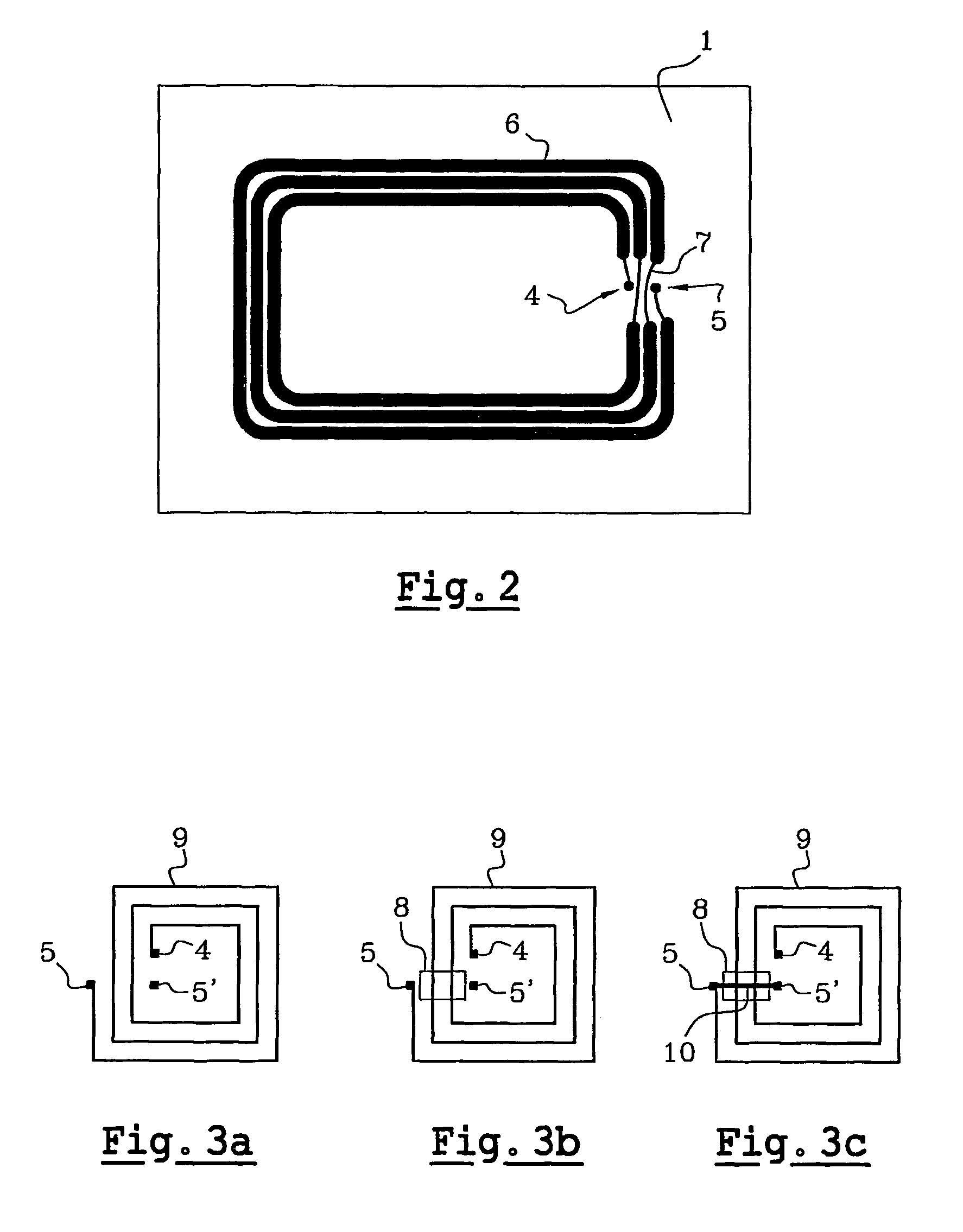
[0032] shown in FIG. 2, it is planned to narrow the width of the tracks at each of the coils, at least locally, and bring them closer to each other at this level. Thus, each coil has a first portion 6 with a track width greater than that of a second coil portion 7. The second portions 7 are also brought closer to each other. With a gravure printing method, these portions can be brought closer together in this way because it is possible to obtain a track width of about 100 μm, and also an inter-track width of about 100 μm. The ends are thus sufficiently close to each other and the pads of the chip may be superimposed in order to be put into contact. This contact may be made, for example, by means of polymer or metal bumps deposited on the pads of the chip in order to connect the ends. In this case, the chip-antenna unit is then surrounded by a resin to protect the connection. In one variant, an anisotropic conductive film (ACF) or an anisotropic conductive paste (ACP), whose electric...

second embodiment

[0033] shown in FIGS. 3a, 3b and 3c, it may be planned to bring these two ends together by making a “bridge” to bring the second end close to the vicinity of the first one. In this case, to enable the second end to go above the coils, an insulating layer 8 is placed between these tracks and the second end. In this case, during a first run, the first end 4, first end 4 forming an internal pad, and an unconnected pad 5′ juxtaposed with the internal pad 4 are formed. The second end 5 forms an external pad and is not connected to the unconnected pad 5′. The antenna 9 planned in this embodiment is not yet obtained. Then, the insulating layer 8 is deposited and, finally, during a second run, the conductive bridge 10 connecting the external pad 5 of the antenna 9 with the unconnected pad 5′ is made. The bridge 10 goes above the insulating layer 8. Thus the second end 5 may be brought inside the smallest coil, in the vicinity of the first end 4. The two runs may be made serially by means of...

third embodiment

[0034] wherein the two faces of the carrier substrate may be used, it is planned to place a module containing the chip on that side of the substrate which does not have the tracks of the printed circuit. This module is then mechanically gripped on this face in such a way that it comes into contact with the ends of the antenna brought to the other face. However, this technique requires that the carrier substrate of the antenna should not be excessively thick, and that it should have a thickness at most equal to 50 μm.


PUM

PropertyMeasurementUnit
Thicknessaaaaaaaaaa
Percent by massaaaaaaaaaa
Weightaaaaaaaaaa

Abstract

In a method for the manufacture of a printed circuit on a dielectric carrier (2), in a first step a circuit pattern (1) is applied with an electrically conductive ink and, in a second step, the circuit model is plated, the electrically conductive ink being applied by means of a method of gravure printing and the plating being done by electrolytic or chemical means.

Description

FIELD OF THE INVENTION[0001]The invention relates to a method for the manufacture of a printed circuit on a dielectric carrier, in which a circuit pattern has an electrically conductive ink applied to it, and the circuit obtained is then plated. The invention also relates to a planar antenna manufactured by this method, and its use in smart nomadic objects (such as smart cards, electronic labels, circuit for wireless communications or the like).[0002]A method for the manufacture of a printed circuit of the type described here above is known from WO 99 / 52336.BACKGROUND OF THE INVENTION[0003]Cards known as smart cards or chip cards have become prevalent in the field of credit cards, ID cards or the like. These are cards in which data pertaining to the user can be stored. Smart cards of this kind have flat contacts on one face. These flat contacts are put into mechanical contact with corresponding contacts in a smart card reader, for the reading or writing of information. The interroga...

Claims


Application Information

Patent Timeline
IPC IPC(8): G03F7/00B41F31/00G06K19/07G06K19/077H05K1/09H05K1/16H05K3/06H05K3/12H05K3/24H05K3/42
CPCG06K19/07779G06K19/07783H05K3/1275H05K3/246H05K1/095H05K1/165H05K3/245H05K2203/1572H05K2201/0347H05K2203/0113H05K2203/0143H05K2203/0534H05K2203/1545H01Q1/38
Inventor MATHIEU, CHRISTOPHE
Owner MICROCONNECTIONS
Learn More