
Reflection-type light modulating array element and exposure apparatus

a light modulating array and array element technology, applied in the field of reflection-type light modulating array element and exposure apparatus, can solve the problems of increased moment of inertia, limited high-speed movement, large mass of the entire movable part, etc., and achieve the effect of enhancing light utility efficiency, small mass and reducing moment of inertia

Inactive Publication Date: 2006-05-16
FUJIFILM HLDG CORP +1
View PDF12 Cites 136 Cited by
  • Summary
  • Abstract
  • Description
  • Claims
  • Application Information

AI Technical Summary

Benefits of technology

The solution enables high-speed and low-voltage driving, miniaturization, and high-resolution performance with improved durability and light utility efficiency by reducing the moment of inertia and increasing electrostatic forces, while simplifying the drive structure and reducing light obstruction.

Problems solved by technology

However, in the spatial light modulator disclosed in JP-A-8-334709, a two-step structure consisting of a yoke part taking a driving role and a mirror part having an area enlarged with respect to the yoke part is constituted on a torsion hinge so as to obtain a high opening ratio for one pixel mirror of a fine area and therefore, the mass of the entire movable part becomes large, as a result, the moment of inertia is increased and high-speed moving is limited.
Furthermore, since the elevated address electrodes and the yoke are coplanarly disposed, the area of each electrode is decreased to give a small electrostatic force both between the pixel mirror and the elevated address electrode and between the yoke and the lower address electrode, and low-voltage and high-speed driving is limited.
In the light deflecting apparatus disclosed in JP-A-2000-214397, the support member (flexible plate) is drawn upward or downward upon displacement of the deflecting plate to cause dogleg bending of the linking part between the flexible plate and the deflecting plate and this gives rise to increase in distortion and reduction in durability.
In the light deflecting apparatus disclosed in Dual-Mode Micromirrors for Optical Phased Array Applications, TRANSDUCERS 01 EUROSENSORS XV, not only the comb drive structure is complicated but also four comb drives are necessary and therefore, a large area is occupied by the drive structure to cause problems that miniaturization and high resolution are difficult to realize and the utility efficiency of light is bad.

Method used


Image

  • Reflection-type light modulating array element and exposure apparatus
  • Reflection-type light modulating array element and exposure apparatus
  • Reflection-type light modulating array element and exposure apparatus

Examples


modification example 1

[0141]FIG. 15 is an enlarged view of the main part of Modification Example 1 where prisms are provided on the microlens array of FIG. 14.

[0142]In this Modification Example, prisms 161 are arrayed to correspond to respective microlenses 115 in the microlens array 113 of the reflection-type light modulating array element 300 in which the light source•SLM unit 129 is provided. The prism 161 ejects the light transmitted through the microlens 115, to the mirror part 57 at a predetermined angle of refraction. The light injected into the mirror part 57 at this angle of refraction is, when the mirror part 67 is at the OFF tilt position, reflected toward the direction different from the injection direction and when the mirror part 57 is at the ON tilt position, reflected to the same direction as the injection direction.

[0143]According to this Modification Example, a prism 161 is provided, so that in the state where the mirror part 57 and the microlens 115 are opposedly disposed, the incident...

modification example 2

[0144]FIG. 16 is an enlarged view of the main point of Modification Example 2 where the incident light to the microlens array is tilted.

[0145]In this Modification Example, the polarizing beam splitter 163 has a polarization splitting surface 163a of reflecting the incident light from the light source at an angle except for right angle. The angle α of the polarization splitting surface 163a is freely set according to the positions of microlenses 115 and reflection-type light modulating elements 100.

[0146]According to this Modification Example, when the angle α of the polarization splitting surface 163a is set to 45° or more, the reflection angle on the polarization splitting surface 163a becomes an obtuse angle and the thickness T of the polarizing beam splitter 163 can be decreased. Also, when the angle α of the polarization splitting surface 163a is set to form an incident light path and a reflected light path on adjacent two microlenses 115 and 115, similarly to Modification Examp...

modification example 3

[0147]FIG. 17 is a constitutional view of Modification Example 3 where a microlens array is provided on the light ejection side of the beam splitter.

[0148]In this Modification Example, a third lens array plate 165 is provided on the surface of the polarizing beam splitter 141 on the exposure light ejection side. The third lens array plate 165 converges each light flux reflected from the mirror part 57 and transmitted through the polarizing beam splitter 141.

[0149]According to this Modification Example, the exposure object 121 can be exposed directly by the modulated light and therefore, an optical system close to contact exposure can be constituted.


PUM


Abstract

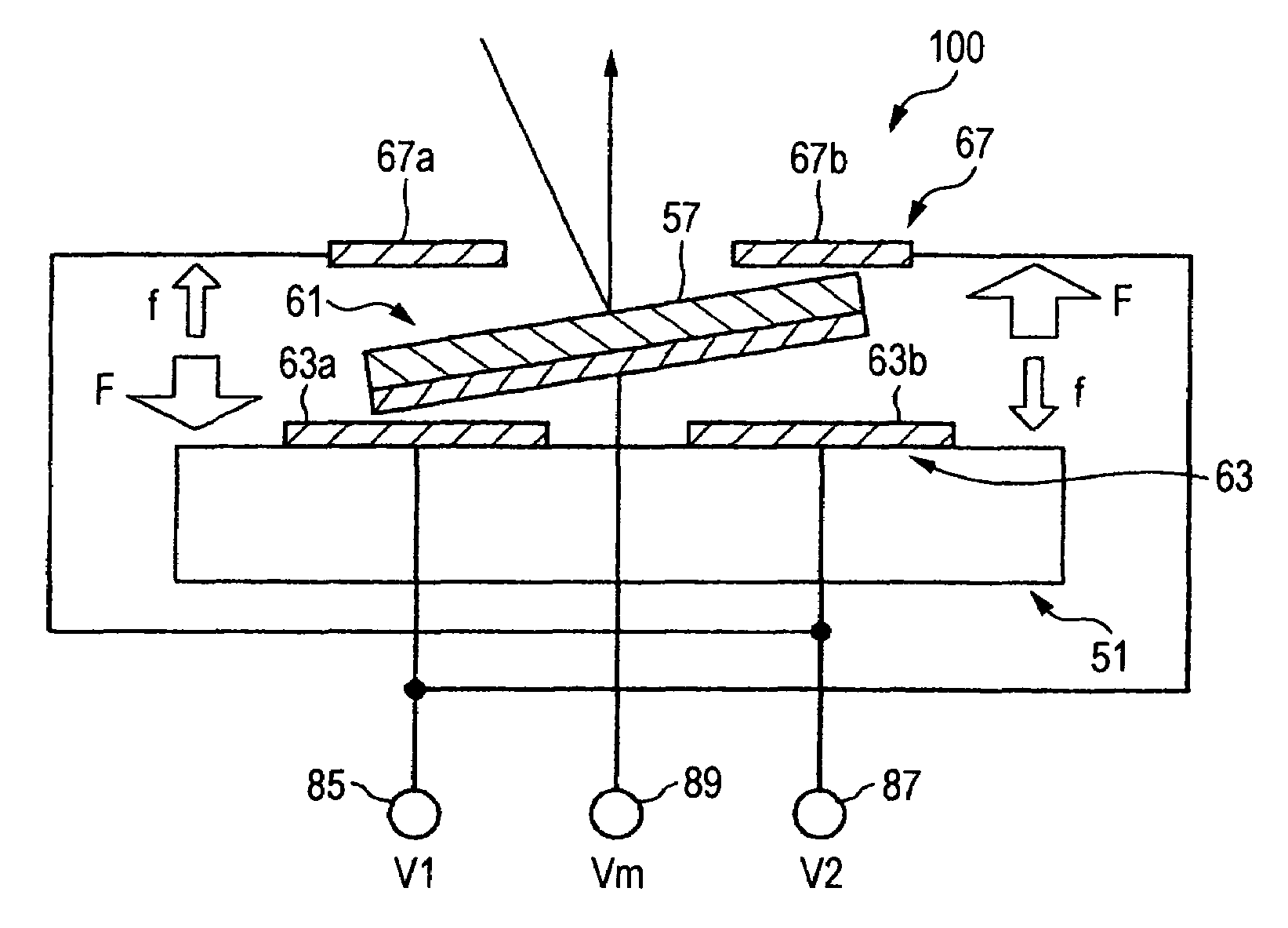
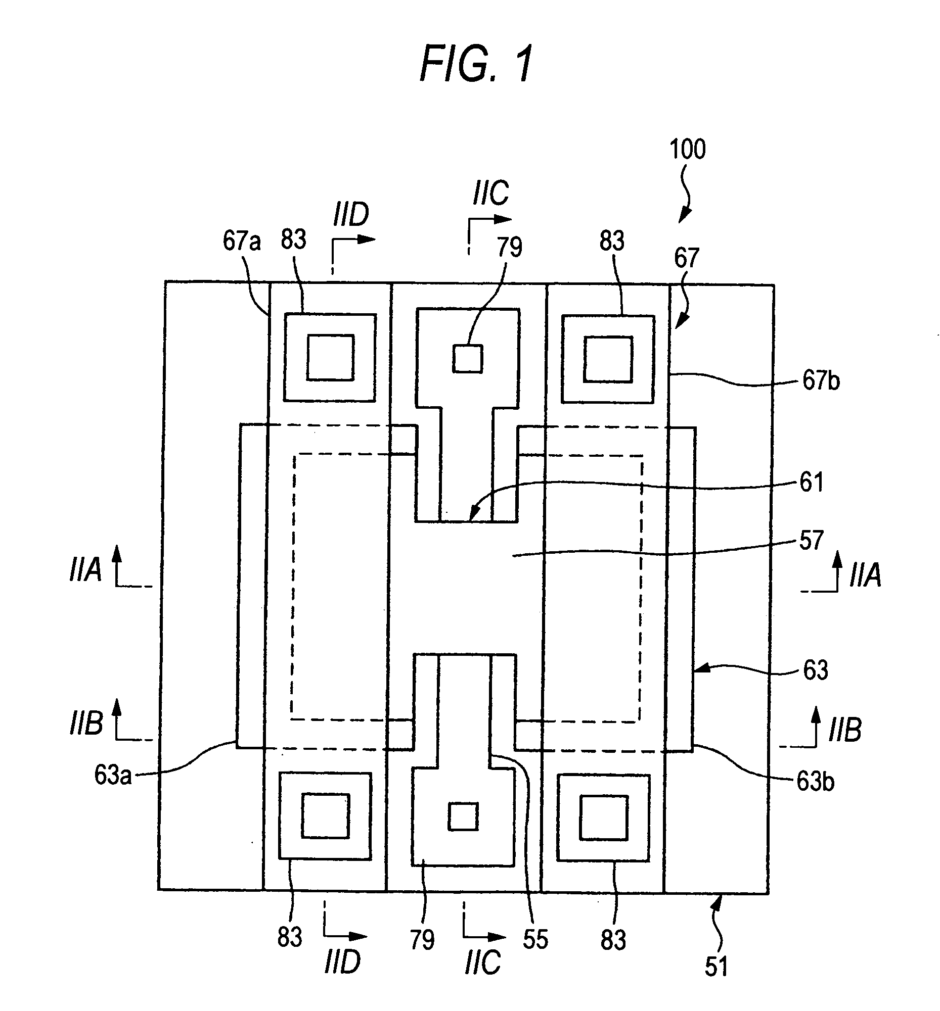
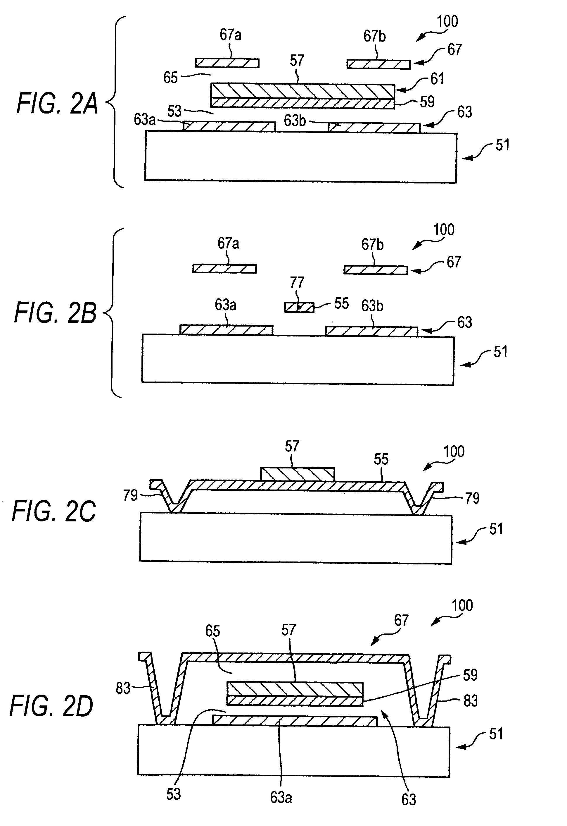
A reflection-type light modulating array element has: a substrate; a movable member provided with a beam body provided on the substrate through a first gap, a light reflector capable of rotational displacement by twisting of the beam body, and an electrically conducting part formed at least in a partial portion of the movable member; a lower electrode provided on a substrate side to face the movable member through the first gap, and an upper electrode provided on a side opposite to the lower electrode to face the movable member through a second gap, and thereby the movable member is between the lower electrode and the upper electrode, wherein a voltage is applied to the upper electrode, the lower electrode and the electrically conducting part to cause an rocking displacement of the light reflector and thereby deflect a reflection direction of a light.

Description

[0001]This application is based on Japanese Patent application JP 2003-356709, filed Oct. 16, 2003, the entire content of which is hereby incorporated by reference.BACKGROUND OF THE INVENTION[0002]1. Technical Field of the Invention[0003]The present invention relates to a reflection-type light modulating array element and an exposure apparatus.[0004]2. Description of the Related Art[0005]The spatial light modulator (SLM) is a device of modulating incident light of a spatial pattern and forming an optical image corresponding to the electrical or optical input. One of SLM is a digital micromirror device (DMD) where a micromirror is produced based on the micromechanic technology and light is deflected by inclining the micromirror. DMD is a monolithic single-chip integrated circuit SLM and comprises, for example, a high-density array of about 16 micron-square movable micromirrors. These mirrors are fabricated over an address circuit and each mirror forms one pixel of the DMD array. This...

Claims


Application Information

Patent Timeline
Patent Type & Authority Patents(United States)
IPC IPC(8): G02B26/00G02B26/08
CPCG02B26/0841
Inventor KIMURA, KOICHISUMI, KATSUTO
Owner FUJIFILM HLDG CORP
Learn More