
Auto black expansion method and apparatus for an image sensor

a technology of image sensor and black expansion method, which is applied in the field of metal oxide semiconductor (mos) image sensor, can solve the problems of difficult to discern objects in areas of low contrast, unsatisfactory fig. 2f, and human observer or operator may not necessarily be interested in very high or very low, so as to reduce the chance of processing errors in a given field

Inactive Publication Date: 2006-05-16
OMNIVISION TECH INC
View PDF5 Cites 2 Cited by
  • Summary
  • Abstract
  • Description
  • Claims
  • Application Information

AI Technical Summary

Benefits of technology

The patent describes a method and apparatus for controlling the auto black expansion and automatic gain control in an image sensor. The method uses black level calibration to eliminate unused signal range and automatic gain control to amplify the video signal at a controlled level. The control system is based on a count of pixel intensities below certain levels, which allows for easier processing and reduces the likelihood of errors. The method also reduces the parts count, wiring requirements, and control circuit complexity. Precise adjustments can be made to the control circuits using a control signal with at least eight bits. The adjustments are made at the end of each field to maintain linear amplification and reduce processing errors.

Problems solved by technology

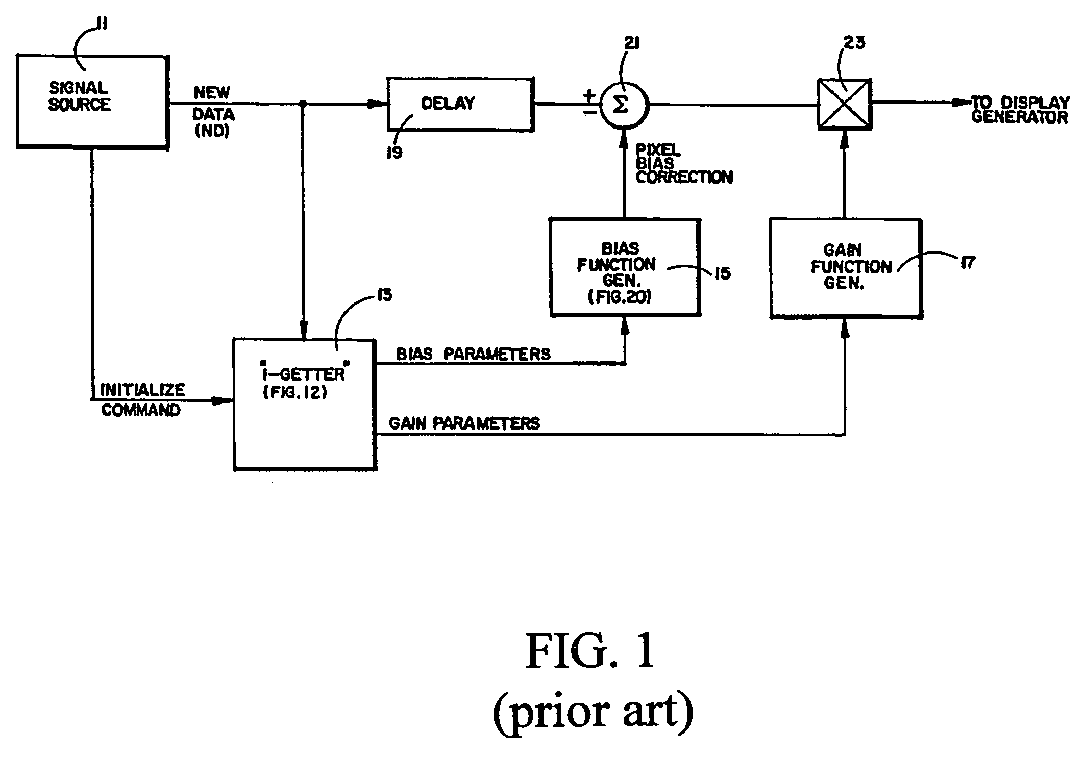
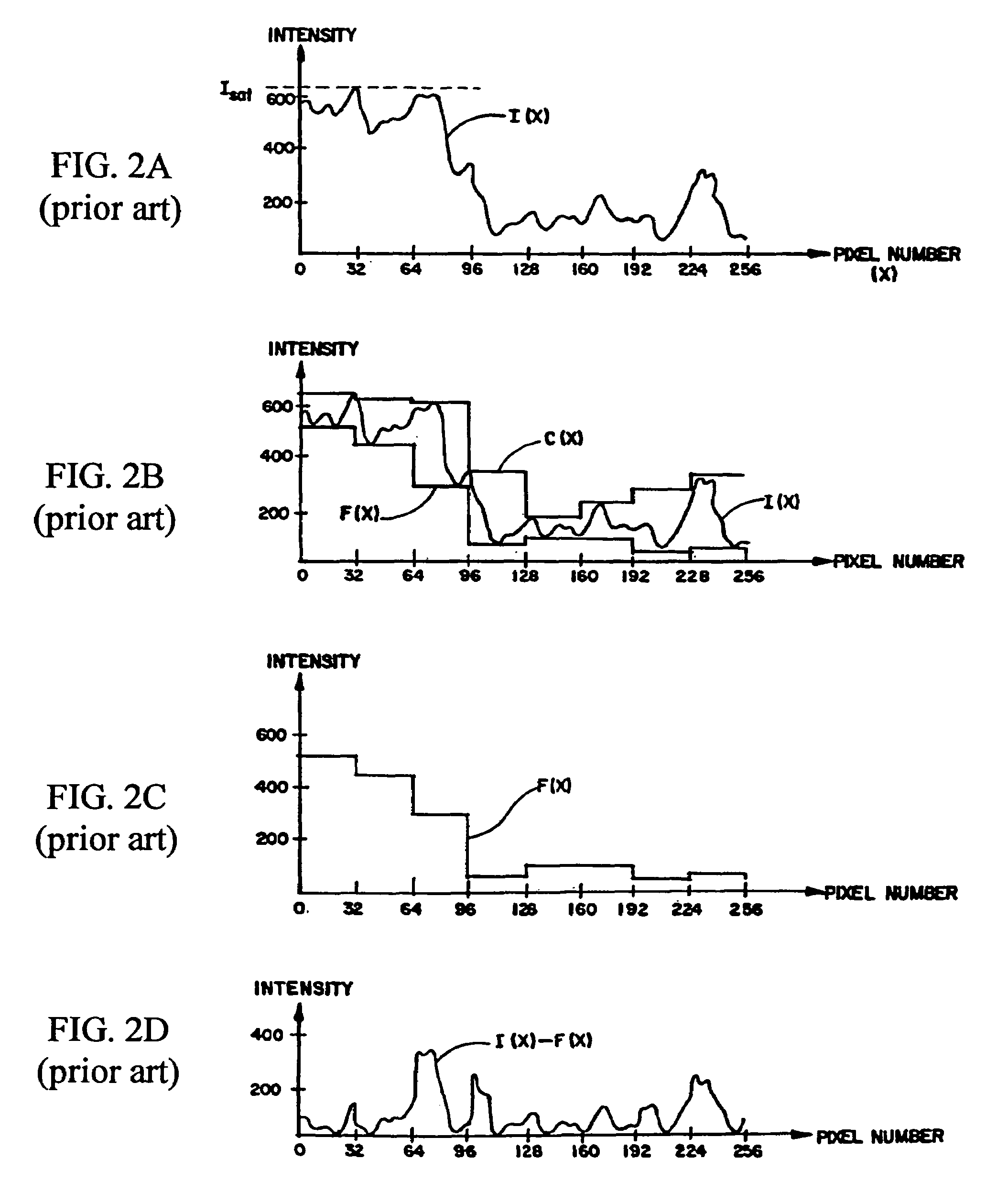
The pixel data at the output of the signal source 11 may have a very narrow dynamic range of contrast, making it extremely difficult to discern objects in areas of lower contrast if directly viewed at the point.
However, a human observer or operator may not necessarily be interested in very high or very low intensity levels in the incoming signal I(x).
However, Vitols et al. describe FIG. 2F as being very unsatisfactory because of the discontinuities or, places where the amplitude of the signal rises or falls vertically.
Although the full dynamic range of the signal is obtained in each data region, the resultant signal shown in FIG. 2F is very bumpy.
So the overall information that an operator may be looking for in the signal may be totally lost in the discontinuities.
One of the drawbacks of the Vitols et al. circuit is that it requires a complex sequence of operations to determine the desired adjustment functions for the system.
In addition, as further described in Vitols et al., it takes time for each of the function generators to get sufficient parameter data in before the function generators can start computing the associated correction signals.

Method used


Image

  • Auto black expansion method and apparatus for an image sensor
  • Auto black expansion method and apparatus for an image sensor
  • Auto black expansion method and apparatus for an image sensor

Examples


Embodiment Construction

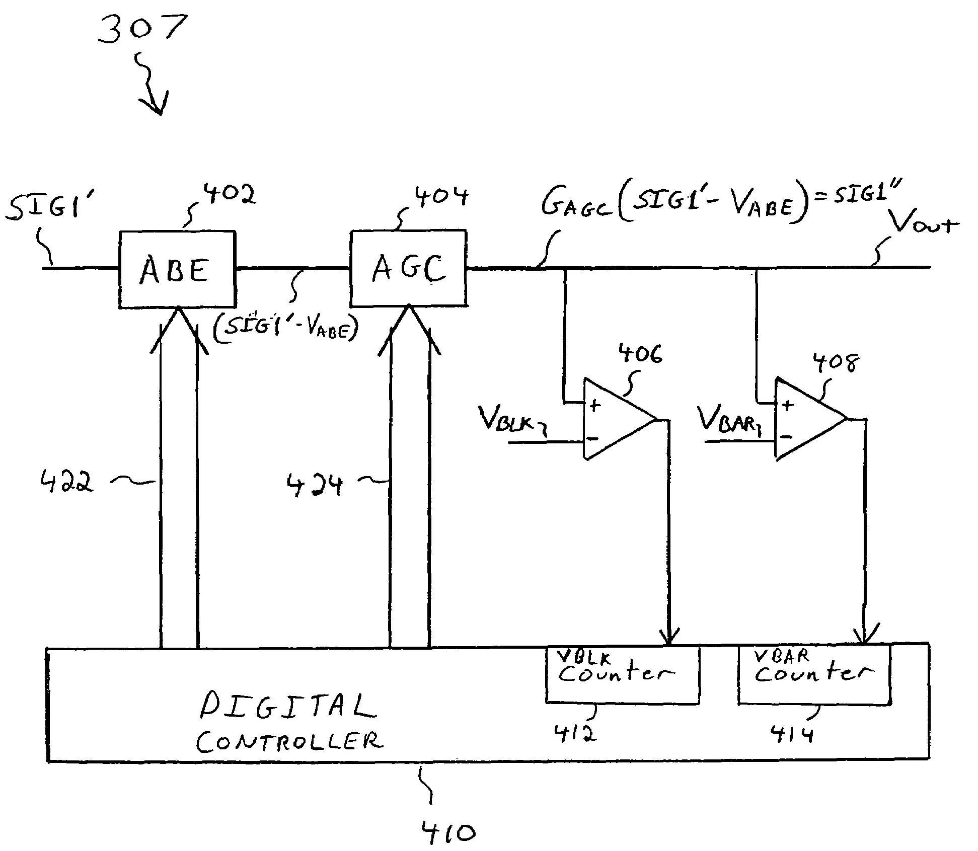
[0032]With reference to FIG. 3, black level calibration and automatic gain control circuiting are shown for use in a single-chip CMOS imaging sensor. The automatic gain control amplification and black level calibration are performed according to the black level expansion method of the present invention. As will be explained in more detail below, the novel method auto black expansion uses a simplified digital control method for the signal processing. The black level calibration attempts to eliminate the portion of the signal that exists when no light is being detected, as is known in the art, thus allowing for a truer zero reference signal so that the later signal processing is improved. The automatic gain control amplifiers (AGC) amplify the signals at a controlled level for further processing.

[0033]As illustrated in FIG. 3, an auto black expansion circuit 402 performs the black level calibration and the automatic gain control circuit 404 performs the gain adjustment. A signal SIG1′...


PUM


Abstract

Auto black expansion circuitry with a simplified digital control system. According to the system, a count of the number of pixels that fall below desired black level and mid-level ranges are maintained. The pixel counts are obtained by comparators that receive the adjusted signals at one input and the desired comparator signal levels at the other input. At the end of a field, when the pixel counts are complete, adjustment to the auto black expansion may be made for the following field. Once the pixel count at the end of a given field indicates that the auto black expansion has achieved the desired level, the automatic gain control may be adjusted for the following field. The method uses single comparators and single counters to obtain the pixel counts. The digital controller outputs an 8-bit control signal to adjust the analog auto black expansion and automatic gain control circuits to precise levels.

Description

FIELD OF THE INVENTION[0001]The present invention relates to metal oxide semiconductor (MOS) image sensors and, more particularly, to auto black expansion systems in such image sensors.BACKGROUND OF THE INVENTION[0002]Integrated circuit technology has revolutionized various fields, including computers, control systems, telecommunications, and imaging. One field in which integrated circuitry is widely used is video imaging. Different types of semiconductor imagers include: charge coupled devices, photodiode arrays, charge injection devices, and hybrid focal plane arrays. Many of these devices include pixels that are arranged in sensor arrays to convert light images into electrical signals.[0003]Examples of MOS imaging devices are detailed in “A ¼ Inch Format 250K Pixel Amplified MOS Image Sensor Using CMOS Process” by Kawashima et al., IEDM 93–575 (1993), and “A Low Noise Line-Amplified MOS Imaging Devices” by Ozaki et al., IEEE Transactions on Electron Devices, Vol. 38, No. 5, May 1...

Claims


Application Information

Patent Timeline
Patent Type & Authority Patents(United States)
IPC IPC(8): H04N5/235H04N5/217H04N5/361H04N5/374
CPCH04N5/361H04N25/63H04N25/671
Inventor DONG, KIMBLECHEN, DATONG
Owner OMNIVISION TECH INC
Learn More