
Method of fabricating sub-micron structures in transparent dielectric materials

a dielectric material and sub-micron technology, applied in the field of microstructure fabrication, can solve the problems of difficult to achieve the fabrication of waveguides that extend from the surface deep into the substrate, cannot be used to form low-loss optical waveguides, and severely restrict the distance between the lens and the irradiated zone, etc., to achieve the effect of small width, increased width and different symmetry

Inactive Publication Date: 2006-04-25
NAT RES COUNCIL OF CANADA
View PDF8 Cites 79 Cited by
  • Summary
  • Abstract
  • Description
  • Claims
  • Application Information

AI Technical Summary

Benefits of technology

[0022]A microstructure typically has channels with sub-micron diameters, although the diameters could extend into the micron range, and, for example, be several microns. An important advantage of the invention, however, is that it is capable of creating structures with sub-micron lateral dimensions but with depths of microns.
[0023]A femtosecond is 10−15 seconds. A femtosecond laser generates pulses in the femtosecond range. The femtosecond laser used by the inventors typically had a pulse duration of 30–40 femtoseconds. However, similar performance for fabricating microstructures can be anticipated for pulse durations on either side of this value e.g. 20 fs to150 fs.
[0024]The laser beam can be fixed relative to the sample. In this case, the laser dosage is the product of the energy per pulse times the number of pulses delivered to the modified zone. It is typically varied in the range determined by altering the energy per laser pulse from 0.01 to 3 μJ and the number of shots between 500 and 5000.
[0025]Alternatively, the beam can be displaced relative to the sample. In this case, where the sample is scanned as it is being irradiated, dosage refers to the cumulative energy per micron of translation and is the product of the energy / pulse times the repetition rate of the laser and divided by the scan rate. The dosage in typically varies in the range determined by the energy per pulse from 0.01 to 1 μJ; the repetition rate from 10–250 kHz and the scan rate from 10–200 μm / s.
[0026]Preferably, the tapered modified zone is located inside the material so that the laser intensity near the surface is too low to modify the surface, and etching takes place from the tip of the tapered zone so that as said selective etching proceeds longitudinally into said modified region, the progressively increasing width of said tapered zone compensates for lateral etching occurring at said narrow end. However, a tapered zone near the top surface can be used in certain applications, for example, in microfluidic applications, to create tapered holes, for use, for example, as nozzles.
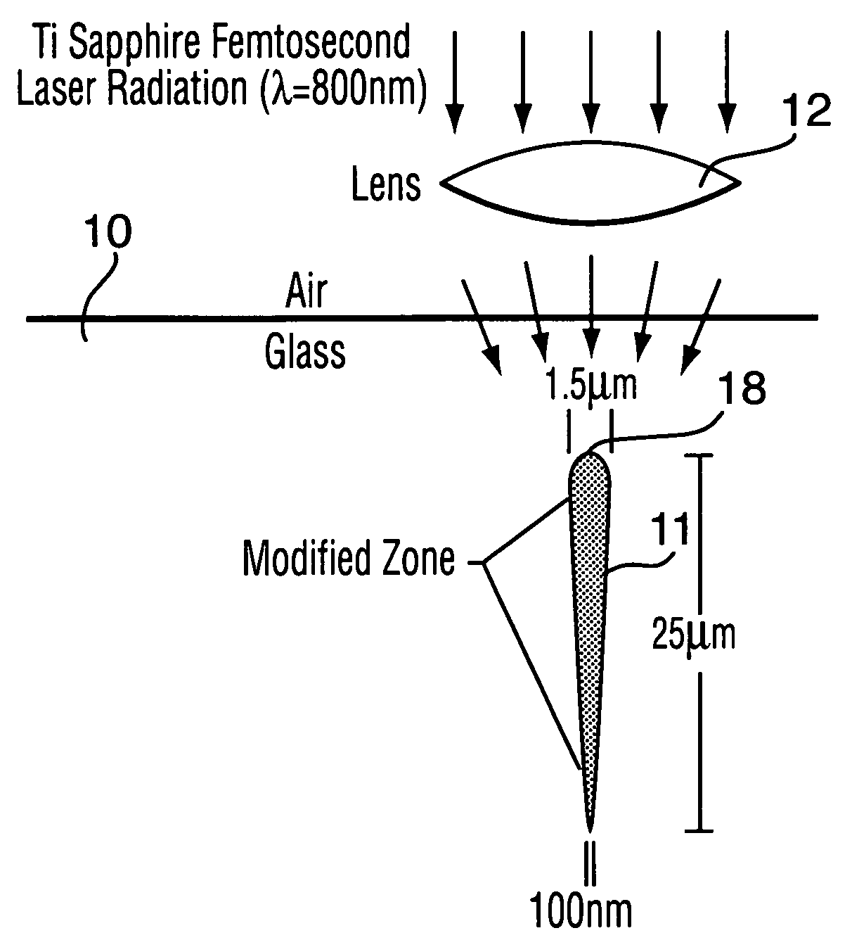
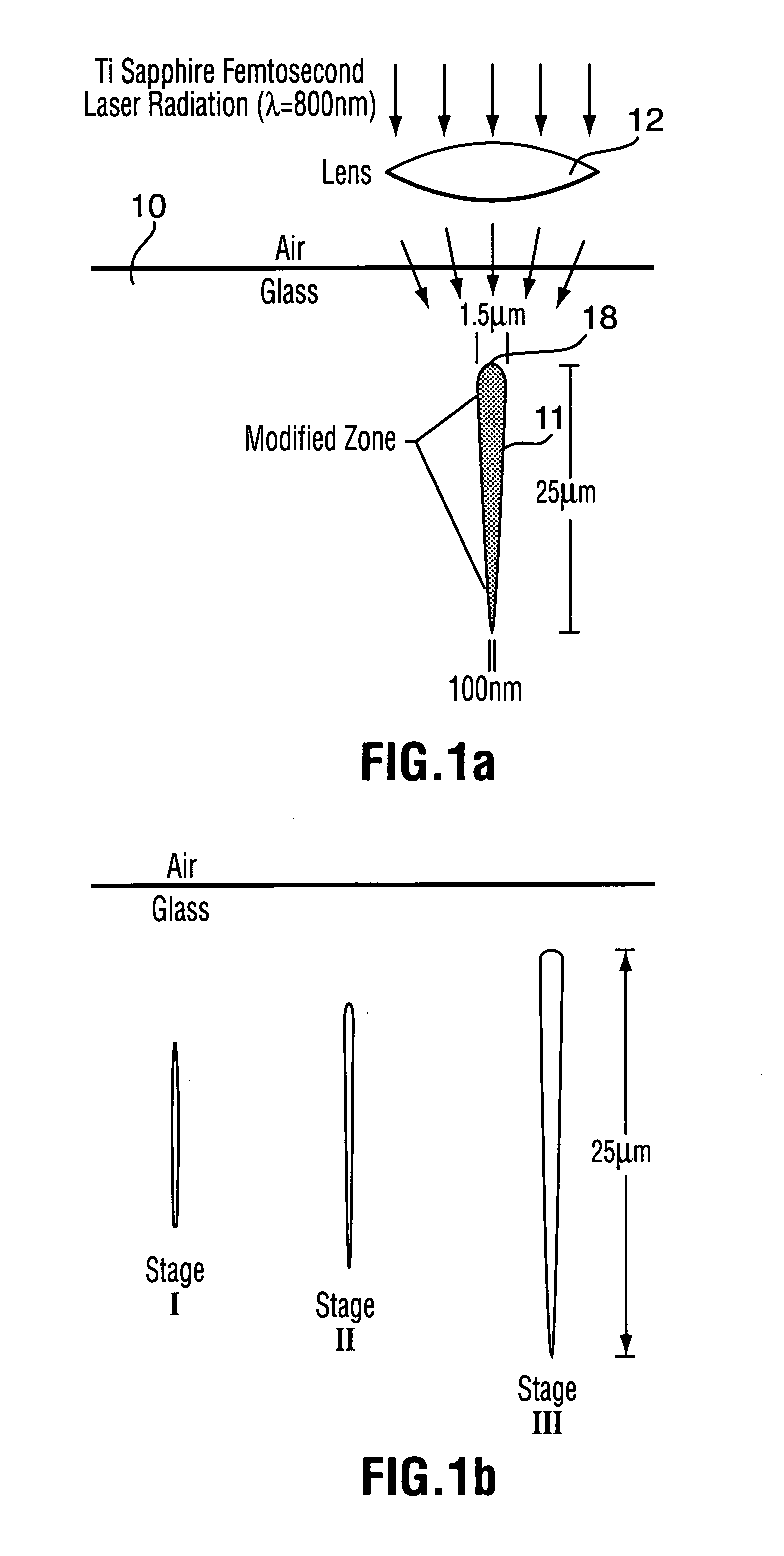
[0027]The invention is based in part on the discovery that the amplified femtosecond laser pulses appropriately focused into a dielectric material create a conical zone of modified material having sufficient length, taper angle and degree of material modification such that when the conical structure is placed near the bottom surface of the bulk dielectric (i.e. the narrow tip region of the conical structure is near the bottom surface) and chemically etched, it produces steep sidewall, sub-micron wide holes or channels.

Problems solved by technology

The “voxels” are highly damaged zones of modified silica and cannot be used to form low loss optical waveguides.
The use of such high NA objectives also severely restricts the distance between the lens and the irradiated zone (e.g. a few hundred microns).
The fabrication of a waveguide that extends from the surface deep into the substrate is difficult to accomplish with conventional microfabrication techniques.
It is believed that no-one has successfully made a practical 2-D photonic crystal band gap structure for telecom wavelengths in bulk glass with any of the above techniques.
The construction of 3-D photonic band-gap structures is considerably more difficult and has met with limited success.
State of the art laser drilling or laser induced dielectric modification followed by chemical etching techniques have not been able to produce clean, deep, sub-micron wide holes or channels in transparent dielectric materials.
It has also not been possible to make an adjoining waveguide to the channel or hole.
It requires access to sophisticated laboratories, which are not always available and are costly to setup.

Method used


Image

  • Method of fabricating sub-micron structures in transparent dielectric materials
  • Method of fabricating sub-micron structures in transparent dielectric materials
  • Method of fabricating sub-micron structures in transparent dielectric materials

Examples


example 1

Fabrication of Photonic Components: A Variable Optical Attenuator

[0083]The combination of a channel with an adjoining waveguide can be used to fabricate a temperature controlled variable attenuator for telecom applications as shown in FIGS. 5a to 5c. In this application a channel 20 created by femtosecond laser writing followed by selective chemical etching (FIG. 5(b)) is partially filled with a polymer 21 (FIG. 5(c)) whose index of refraction is less than that of the waveguide core and which has a temperature dependent absorption at e.g. λ=1.5 μm. The polymer 21 could also be from a class of polymers with large thermo-optical responses leading to large index of refraction changes as the polymer is heated. The index gradients can be made sufficiently large to deflect light out of the waveguide.

[0084]A metal coating 22 is subsequently deposited on top of the polymer and the entire surface is polished to remove the metal and polymer everywhere except in the channels. The small cross-s...

example 2

Microfluidic Applications on a Silica Chip

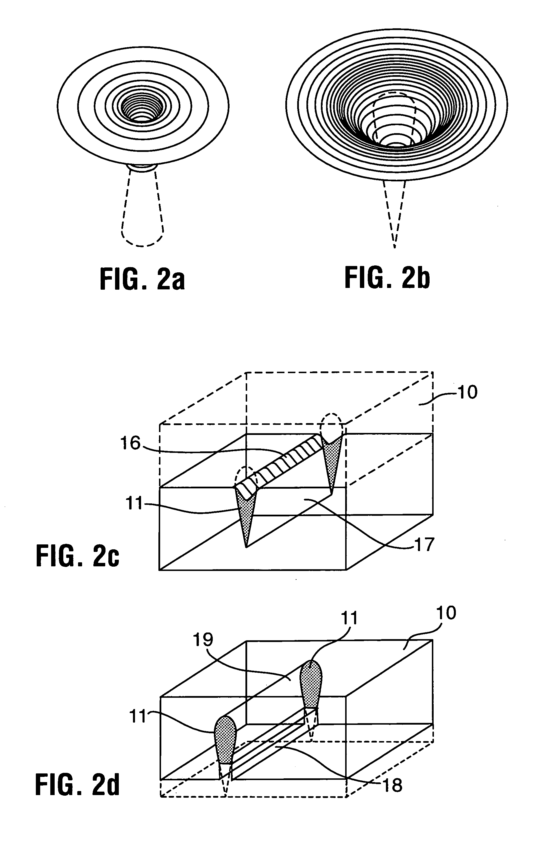
[0086]The method in accordance with the invention permits the production of precise channels, which can be tapered and formed into complicated patterns such as mixing chambers for chemistry on a chip experiments.

[0087]The value of these narrow channels for chemistry on a chip experiments is enhanced since with each channel there is an adjoining optical waveguide, which can couple light into or out of the channel. One could also use arrays of micron-sized holes to trap very small droplets of liquid for analysis.

[0088]It is also possible to partially coat the interior of the channels / holes with metal. The metal is then removed everywhere except in the channels / holes by polishing. Laser radiation delivered through the waveguides attached to the channels / holes can be absorbed by the metal to control the temperature of samples placed in such channels / holes. The laser radiation can also be used heat the samples sufficiently rapidly to eject the ma...

example 3

Biological Sensing Applications on a Chip

[0089]Very small volumes of biological material can be inserted into the narrow channels where it can be interrogated by light traveling in the waveguide adjoining the channel.

[0090]There are also biological sensor applications for holes and their vertically connected waveguides. For example, biological specimens could be inserted into the holes. An entire array of holes could then be irradiated with UV light and the fluorescence from each specimen could be guided by its own waveguide for selective detection. Alternatively holes containing a sample could be individually irradiated or sampled through its own waveguide.

[0091]It is also possible to use light traveling in a horizontal waveguide, which has no adjoining channel but instead interfaces with a series of holes, to simultaneously irradiate material contained in all of the holes. Light emanating from each hole e.g. fluorescence, can be detected using the dedicated vertical waveguides adj...


PUM

PropertyMeasurementUnit
diameteraaaaaaaaaa
diameteraaaaaaaaaa
thicknessaaaaaaaaaa

Abstract

A sub-micron structure is fabricated in a transparent dielectric material by focusing femtosecond laser pulses into the dielectric to create a highly tapered modified zone with modified etch properties. The dielectric material is then selectively etched into the modified zone from the direction of the narrow end of the tapered zone so that as the selective etching proceeds longitudinally into the modified zone, the progressively increasing width of the modified zone compensates for lateral etching occurring closer to the narrow end so as to produce steep-walled holes. The unetched portion of the modified zone produced by translating the laser beam close to and parallel to the bottom surface of the dielectric can serve as an optical waveguide to collect light from or deliver light to the etched channel which can contain various biological, optical, or chemical materials for sensing applications.

Description

CROSS REFERENCE TO RELATED APPLICATION[0001]This application claims the benefit under 35 USC 119(e) of U.S. provisional application No. 60 / 319,236 filed May 8, 2002.FIELD OF THE INVENTION[0002]This invention relates to the field of microstructure fabrication, and in particular to a method of fabricating sub-micron structures in transparent dielectric materials.BACKGROUND OF INVENTION[0003]There is a need to integrate materials with optical waveguides for both sensing applications as well as a means to alter the properties of the propagating light. The integration can include, for example, biological and chemical samples, polymers, liquid crystals as well as non-linear optical and modulator materials. Such integration can benefit from the manufacture of dense arrays of sub-micron wide, high aspect ratio holes (with attoliter volumes; 1 attoliter=10−18 liters)or channels in dielectric materials, such as glass which are interfaced directly with adjoining optical waveguides for light de...

Claims


Application Information

Patent Timeline
Patent Type & Authority Patents(United States)
IPC IPC(8): C03C25/68B81C99/00G02B6/02G02B6/12G02B6/13G02B6/136G02F1/01G02F1/065
CPCG02F1/065G02B6/136G02B6/13G02B6/02285G02B6/02371G02B6/02385G02F1/0147
Inventor TAYLOR, RODHNATOVSKY, CYRILCORKUM, PAULRAYNER, DAVIDBHARDWAJ, RAVI
Owner NAT RES COUNCIL OF CANADA
Learn More